SCEA046A September 2011 – November 2022 CD54HC14 , CD54HCT14 , CD74AC14 , CD74ACT14 , CD74HC14 , CD74HCT14 , SN5414 , SN5417 , SN54AC14 , SN54ACT14 , SN54AHC14 , SN54AHCT14 , SN54HC14 , SN54HCT14 , SN54LS14 , SN7414 , SN7417 , SN74AC14 , SN74ACT14 , SN74AHC14 , SN74AHC1G14 , SN74AHCT14 , SN74AHCT1G14 , SN74ALVC14 , SN74AUC14 , SN74AUC17 , SN74AUC1G14 , SN74AUC1G17 , SN74AUP1G00 , SN74AUP1G02 , SN74AUP1G04 , SN74AUP1G06 , SN74AUP1G07 , SN74AUP1G08 , SN74AUP1G125 , SN74AUP1G126 , SN74AUP1G14 , SN74AUP1G17 , SN74AUP1G17-EP , SN74AUP1G240 , SN74AUP1G32 , SN74AUP1G34 , SN74AUP1G57 , SN74AUP1G58 , SN74AUP1G74 , SN74AUP1G79 , SN74AUP1G80 , SN74AUP1G97 , SN74AUP1G98 , SN74AUP1G99 , SN74AUP1T00 , SN74AUP1T02 , SN74AUP1T04 , SN74AUP1T08 , SN74AUP1T14 , SN74AUP1T157 , SN74AUP1T158 , SN74AUP1T17 , SN74AUP1T32 , SN74AUP1T57 , SN74AUP1T58 , SN74AUP1T86 , SN74AUP1T87 , SN74AUP1T97 , SN74AUP1T98 , SN74AUP2G00 , SN74AUP2G00-Q1 , SN74AUP2G02 , SN74AUP2G04 , SN74AUP2G06 , SN74AUP2G07 , SN74AUP2G08 , SN74AUP2G125 , SN74AUP2G126 , SN74AUP2G14 , SN74AUP2G17 , SN74AUP2G240 , SN74AUP2G241 , SN74AUP2G32 , SN74AUP2G34 , SN74AUP2G79 , SN74AUP2G80 , SN74AUP3G04 , SN74AUP3G06 , SN74AUP3G07 , SN74AUP3G14 , SN74AUP3G17 , SN74AUP3G34 , SN74HC14 , SN74HCT14 , SN74LS14 , SN74LVC1G14 , SN74LVC1G17 , SN74LVC1G57 , SN74LVC1G58 , SN74LVC1G97 , SN74LVC1G97-EP , SN74LVC1G97-Q1 , SN74LVC1G98 , SN74LVC1G98-EP , SN74LVC1G98-Q1 , SN74LVC1G99 , SN74LVC1G99-Q1 , SN74LVC1GU04 , SN74LVC2G14 , SN74LVC2G17 , SN74LVC3G14 , SN74LVC3G17
PRODMIX
1 Application Brief
Most CMOS, BiCMOS and TTL devices require fast edges on the high and low transitions of their inputs. If the edges are too slow, they can cause excessive current, oscillation, or may damage the device.
Slow or Noisy Edges
Slow edges are sometimes hard to avoid at power-up or when using push-button or manual switches with the large capacitors needed for filtering. Heavily loaded outputs can also cause input rise and fall time to be out of specification for the next part down the line. On a normal (non-Schmitt trigger) input, the part will switch at the same point on the rising edge and falling edge. With a slow rising edge the part will switch at the threshold. When the switch occurs, it will require current from Vcc.
When current is forced from VCC, the VCC level can drop and cause the threshold to shift. When the threshold shifts it will cross the input again causing the part to switch again. This pattern can continue causing oscillation, which can cause excessive current. This pattern can also happen if noise is on the input. The noise can cross the threshold multiple times and cause oscillation or multiple clocking.
Hysteresis
The solution to these problems is to use a Schmitt trigger device to translate the slow or noisy edges into something faster that will meet the input rise and fall specifications of the following device. A true Schmitt trigger does not have rise and fall time limitations.
Parts with Schmitt trigger action have a small amount of hysteresis that helps with noise rejection but still have an input rise and fall time-limit. These parts usually do not have VT specifications in the data sheet and have rise and fall time limitations specified for the inputs in the recommended operating conditions.
The true Schmitt trigger input has the switching threshold adjusted where the part will switch at a higher point (Vt+) on the rising edge and at a lower point (Vt–) on the falling edge. The difference in these switching points is called Hysteresis (^Vt). Here is an example of Schmitt trigger specs:
| PARAMETER | Vcc | MIN | MAX | UNIT |
|---|---|---|---|---|
| VT+ (Positive-going input threshold voltage) | 1.65 V | 0.76 | 1.13 | V |
| 2.3 V | 1.08 | 1.56 | ||
| 3 V | 1.48 | 1.92 | ||
| 4.5 V | 2.19 | 2.74 | ||
| 5.5 V | 2.65 | 3.33 | ||
| VT– (Negative-going input threshold voltage) | 1.65 V | 0.35 | 0.59 | V |
| 2.3 V | 0.56 | 0.88 | ||
| 3 V | 0.89 | 1.2 | ||
| 4.5 V | 1.51 | 1.97 | ||
| 4.5 V | 1.88 | 2.4 | ||
| ΔVT Hysteresis (VT+ – VT–) | 1.65 V | 0.36 | 0.64 | V |
| 2.3 V | 0.45 | 0.78 | ||
| 3 V | 0.51 | 0.83 | ||
| 4.5 V | 0.58 | 0.93 | ||
5.5 V | 0.69 | 1.04 |
It is important to remember (Vt+ max) = Vih and (VT– min) = Vil. In the specs, multiple limits are related to the Schmitt trigger inputs. All of the limits are important for different reasons. On the input rising edge, the part will switch between (Vt+ min) and (Vt+ max). On the falling edge, the part will switch between (Vt– max) and (Vt– min). The part will not switch between (Vt– max) and (Vt+ min). This is important for noise rejection.
The hysteresis is the delta between where the part switches on the rising edge and where it switches on the falling edge. The hysteresis will be at least the min and no more than the max (^Vt) spec.
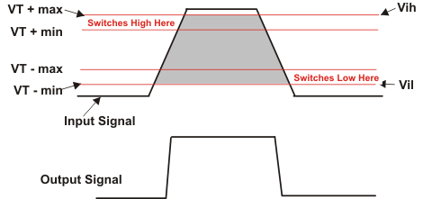 Figure 1-1 .
 Input Voltage
One common misconception is that the current consumption will be less when switching a slow signal into a Schmitt trigger. This misconception is partly true because the Schmitt trigger prevents oscillation which can draw a lot of current; however, the Icc current may still be higher due to the amount of time the input is not at the rail. This is Delta Icc. Delta Icc is where the inputs are not at the rails and upper or lower drive transistors are partially on. The plot below shows Icc across the input voltage sweep.
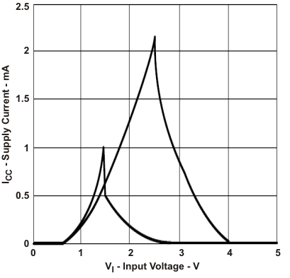 Figure 1-2 Supply Current as a Function of Input Voltage
Sine Waves
Use Schmitt triggers to translate a sine wave into a square wave as shown in this oscillator application. Also, use Schmitt triggers to speed up a slow or noisy input, or clean up an input, as in the switch de-bouncer circuit.
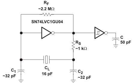 Figure 1-3 Oscillator Application
Using Schmitt Trigger Inverter
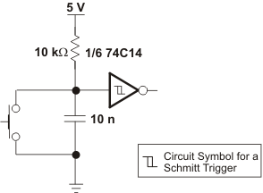 Figure 1-4 Switch De-bouncer Using Schmitt Trigger Inverter.
 Conclusion
Schmitt triggers can be used to change a sine wave into a square wave, clean up noisy signals, and convert slow edges to fast edges.
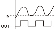 Figure 1-5 Sine Wave to Square
Wave.
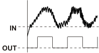 Figure 1-6 Clean Noisy Signals.
  Figure 1-7 Convert Slow Edges.
 We specify the part will switch on the rising edge between (VT+ min) and (VT+ max). We specify the part will switch on the falling edge between (VT– max) and (VT– min).
Between (VT+ min) and (VT– max), we specify the part will not switch. This specification can be used for noise rejection. These 2 limits can overlap.
We specify a minimum amount of hysteresis as delta VT min.
Vih = (VT+ max)
Vil = (VT– min)
Texas Instrument Schmitt trigger functions are available in most all technology families from the 30 year old 74XX family to the latest AUP1T family. These two Schmitt-trigger functions are available in most families:
14 for inverting Schmitt trigger
17 for non-inverting Schmitt trigger
Texas Instrument also has a complete line of little logic products with Schmitt trigger inputs.
Configurations
SN74LVC1G57, SN74LVC1G58, SN74LVC1G97, SN74LVC1G98, SN74LVC1G99 SN74AUP1G57, SN74AUP1G58, SN74AUP1G97, SN74AUP1G98, SN74AUP1G99
Low to High Translators
SN74AUP1T02, SN74AUP1T04, SN74AUP1T08, SN74AUP1T14, SN74AUP1T157, SN74AUP1T158, SN74AUP1T17, SN74AUP1T32, SN74AUP1T86