SNVS521K December 2007 – August 2014 LP2998 , LP2998-Q1
PRODUCTION DATA.
- 1 Features
- 2 Applications
- 3 Description
- 4 Simplified Schematic
- 5 Revision History
- 6 Pin Configuration and Functions
- 7 Specifications
- 8 Detailed Description
- 9 Application and Implementation
- 10Power Supply Recommendations
- 11Layout
- 12Device and Documentation Support
- 13Mechanical, Packaging, and Orderable Information
パッケージ・オプション
メカニカル・データ(パッケージ|ピン)
- DDA|8
サーマルパッド・メカニカル・データ
- DDA|8
発注情報
1 Features
- AEC-Q100 Test Guidance with the following results (SO PowerPAD-8):
- Device HBM ESD Classification Level H1C
- Junction Temperature Range –40°C to 125°C
- 1.35 V Minimum VDDQ
- Source and Sink Current
- Low Output Voltage Offset
- No External Resistors Required
- Linear Topology
- Suspend to Ram (STR) Functionality
- Low External Component Count
- Thermal Shutdown
2 Applications
- DDR1, DDR2, DDR3, and DDR3L Termination Voltage
- Automotive Infotainment
- FPGA
- Industrial/Medical PC
- SSTL-18, SSTL-2, and SSTL-3 Termination
- HSTL Termination
3 Description
The LP2998 linear regulator is designed to meet JEDEC SSTL-2 and JEDEC SSTL-18 specifications for termination of DDR-SDRAM and DDR2 memory. The device also supports DDR3 and DDR3L VTT bus termination with VDDQ min of 1.35 V. The device contains a high-speed operational amplifier to provide excellent response to load transients. The output stage prevents shoot through while delivering 1.5 A continuous current and transient peaks up to 3 A in the application as required for DDR-SDRAM termination. The LP2998 also incorporates a VSENSE pin to provide superior load regulation and a VREF output as a reference for the chipset and DIMMs.
An additional feature found on the LP2998 is an active low shutdown (SD) pin that provides Suspend To RAM (STR) functionality. When SD is pulled low the VTT output will tri-state providing a high impedance output, but, VREF will remain active. A power savings advantage can be obtained in this mode through lower quiescent current.
Device Information(1)
| PART NUMBER | PACKAGE | BODY SIZE (NOM) |
|---|---|---|
| LP2998 | SO PowerPAD™ (8) | 4.89 mm x 3.90 mm |
| LP2998 | SOIC (8) | 4.90 mm x 3.91 mm |
| LP2998-Q1 | SO PowerPAD™ (8) | 4.89 mm x 3.90 mm |
- For all available packages, see the orderable addendum at the end of the datasheet.
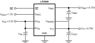
4 Simplified Schematic
