SCES323Q June 2001 – March 2017 SN74LVC1G66
PRODUCTION DATA.
- 1 Features
- 2 Applications
- 3 Description
- 4 Revision History
- 5 Pin Configuration and Functions
- 6 Specifications
- 7 Parameter Measurement Information
- 8 Detailed Description
- 9 Application and Implementation
- 10Power Supply Recommendations
- 11Layout
- 12Device and Documentation Support
- 13Mechanical, Packaging, and Orderable Information
Package Options
Refer to the PDF data sheet for device specific package drawings
Mechanical Data (Package|Pins)
- DBV|5
- DSF|6
- DCK|5
- DRL|5
- DRY|6
- YZP|5
Thermal pad, mechanical data (Package|Pins)
- DRY|6
Orderable Information
1 Features
- Available in the Texas Instruments NanoFree™ Package
- 1.65-V to 5.5-V VCC Operation
- Inputs Accept Voltages to 5.5 V
- Max tpd of 0.8 ns at 3.3 V
- High On-Off Output Voltage Ratio
- High Degree of Linearity
- High Speed, Typically 0.5 ns (VCC = 3 V,
CL = 50 pF) - Low ON-State Resistance, Typically ≉5.5 Ω (VCC = 4.5 V)
- Latch-Up Performance Exceeds 100 mA Per JESD 78, Class II
- ESD Protection Exceeds JESD 22
- 2000-V Human-Body Model (A114-A)
- 200-V Machine Model (A115-A)
- 1000-V Charged-Device Model (C101)
2 Applications
- Wireless Devices
- Audio and Video Signal Routing
- Portable Computing
- Wearable Devices
- Signal Gating, Chopping, Modulation or Demodulation (Modem)
- Signal Multiplexing for Analog-to-Digital and Digital-to-Analog Conversion Systems
3 Description
This single analog switch is designed for 1.65-V to 5.5-V VCC operation.
The SN74LVC1G66 device can handle analog and digital signals. The device permits bidirectional transmission of signals with amplitudes of up to 5.5 V (peak).
NanoFree package technology is a major breakthrough in IC packaging concepts, using the die as the package.
Device Information(1)
| PART NUMBER | PACKAGE | BODY SIZE (NOM) |
|---|---|---|
| SN74LVC1G66DBV | SOT-23 (5) | 2.90 mm × 1.60 mm |
| SN74LVC1G66DCK | SC70 (5) | 2.00 mm × 1.25 mm |
| SN74LVC1G66DRL | SOT (5) | 1.60 mm × 1.20 mm |
| SN74LVC1G66DRY | SON (6) | 1.45 mm × 1.00 mm |
| SN74LVC1G66YZP | DSBGA (5) | 1.39 mm × 0.89 mm |
| SN74LVC1G66DSF | SON (6) | 1.00 mm x 1.00 mm |
- For all available packages, see the orderable addendum at the end of the datasheet.
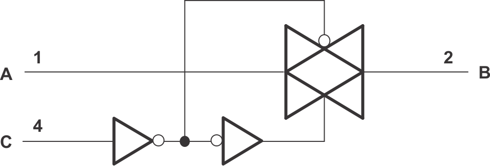
Logic Diagram (Positive Logic)
