SLUS769D July 2013 – December 2016 UCC28910 , UCC28911
PRODUCTION DATA.
- 1 Features
- 2 Applications
- 3 Description
- 4 Simplified Schematic
- 5 Revision History
- 6 Device Comparison Table
- 7 Pin Configuration and Functions
- 8 Detailed Pin Description
- 9 Specifications
-
10Detailed Description
- 10.1 Overview
- 10.2 Functional Block Diagram
- 10.3 Feature Description
- 10.4 Device Functional Modes
-
11Applications and Implementation
- 11.1 Application Information
- 11.2
Typical Application
- 11.2.1
Battery Charger, 5 V, 6 W
- 11.2.1.1 Design Requirements
- 11.2.1.2
Detailed Design Procedure
- 11.2.1.2.1 Power Handling Curves
- 11.2.1.2.2 Input Stage Design and Bulk Capacitance
- 11.2.1.2.3 Transformer Turns Ratio
- 11.2.1.2.4 Output Capacitance
- 11.2.1.2.5 VDD Capacitance, CVDD
- 11.2.1.2.6 VS Resistor Divider
- 11.2.1.2.7 RVDD Resistor and Turn Ratio
- 11.2.1.2.8 Transformer Input Power
- 11.2.1.2.9 RIPK Value
- 11.2.1.2.10 Transformer Primary Inductance Value
- 11.2.1.2.11 Pre-Load
- 11.2.1.2.12 DRAIN Voltage Clamp Circuit
- 11.2.2 Application Curves
- 11.2.3 Multi-Output Converter with UCC2891x Devices
- 11.2.4 Do’s and Don'ts
- 11.2.1
Battery Charger, 5 V, 6 W
- 12Power Supply Recommendations
- 13Layout
- 14Device and Documentation Support
- 15Mechanical, Packaging, and Orderable Information
Package Options
Mechanical Data (Package|Pins)
- D|7
Thermal pad, mechanical data (Package|Pins)
Orderable Information
1 Features
- Constant-Voltage (CV) and Constant-Current (CC) Output Regulation Without Optical-Coupler
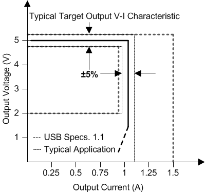
- ±5% Output Voltage Regulation Accuracy
- ±5% Output Current Regulation With AC Line and Primary Inductance Tolerance Compensation
- 700-V Start-Up and Smart Power Management Enables <30-mW Standby Power
- 115-kHz Maximum Switching Frequency Design for High-Power Density
- Valley Switching and Frequency Dithering to Ease EMI Compliance
- Thermal Shut Down
- Low Line and Output Over-Voltage Protection
2 Applications
- Home and Building Automation
- Power Metering Bias
- Bias Power for Smoke Alarm, Fire Alarm and Thermostat
- Wall Adapters, Chargers for Mobile Phones
- Smart plug, IoT, MCU and WiFi Power
- Aux power for TV, Server, White Goods
- LED Lighting
3 Description
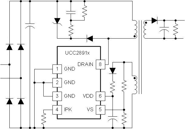
The UCC28910 and UCC28911 are high-voltage flyback switchers that provide output voltage and current regulation without the use of an optical coupler. Both devices incorporate a 700-V power FET and a controller that process operating information from the flyback auxiliary winding and power FET to provide a precise output voltage and current control. The integrated high-voltage current source for startup that is switched off during device operation, and the controller current consumption is dynamically adjusted with load. Both enable the very low stand-by power consumption.
Control algorithms in the UCC28910 and UCC28911, combining switching frequency and peak primary current modulation, allow operating efficiencies to meet or exceed applicable standards. Discontinuous conduction mode (DCM) with valley switching is used to reduce switching losses. Built-in protection features help to keep secondary and primary component stress levels in check across the operating range. The frequency jitter helps to reduce EMI filter cost.
Device Information
| PART NUMBER | PACKAGE | BODY SIZE (NOM) |
|---|---|---|
| UCC28910 | SOIC-7 (7) | 5.00 mm x 6.20 mm |
| UCC28911 | SOIC-7 (7) | 5.00 mm x 6.20 mm |

