SLUSBL7B December 2013 – October 2015 UCC28722
PRODUCTION DATA.
- 1 Features
- 2 Applications
- 3 Description
- 4 Revision History
- 5 Pin Configuration and Functions
- 6 Specifications
- 7 Detailed Description
-
8 Application and Implementation
- 8.1 Application Information
- 8.2
Typical Application
- 8.2.1 Design Requirements
- 8.2.2
Detailed Design Procedure
- 8.2.2.1 Stand-by Power Estimate
- 8.2.2.2 Input Bulk Capacitance and Minimum Bulk Voltage
- 8.2.2.3 Transformer Turns Ratio, Inductance, Primary-Peak Current
- 8.2.2.4 Transformer Parameter Verification
- 8.2.2.5 Output Capacitance
- 8.2.2.6 VDD Capacitance, CDD
- 8.2.2.7 VS Resistor Divider, Line Compensation, and Cable Compensation
- 8.2.2.8 Startup Resistance and Startup Time
- 8.2.3 Application Curves
- 9 Power Supply Recommendations
- 10Layout
-
11Device and Documentation Support
- 11.1
Device Support
- 11.1.1
Device Nomenclature
- 11.1.1.1
Definition of Terms
- 11.1.1.1.1 Capacitance Terms in Farads
- 11.1.1.1.2 Duty Cycle Terms
- 11.1.1.1.3 Frequency Terms in Hertz
- 11.1.1.1.4 Current Terms in Amperes
- 11.1.1.1.5 Current and Voltage Scaling Terms
- 11.1.1.1.6 Transformer Terms
- 11.1.1.1.7 Power Terms in Watts
- 11.1.1.1.8 Resistance Terms in Ω
- 11.1.1.1.9 Timing Terms in Seconds
- 11.1.1.1.10 Voltage Terms in Volts
- 11.1.1.1.11 AC Voltage Terms in VRMS
- 11.1.1.1.12 Efficiency Terms
- 11.1.1.1
Definition of Terms
- 11.1.1
Device Nomenclature
- 11.2 Documentation Support
- 11.3 Community Resources
- 11.4 Trademarks
- 11.5 Electrostatic Discharge Caution
- 11.6 Glossary
- 11.1
Device Support
- 12Mechanical, Packaging, and Orderable Information
Package Options
Mechanical Data (Package|Pins)
- DBV|6
Thermal pad, mechanical data (Package|Pins)
Orderable Information
1 Features
- < 50-mW No-Load Power
- Primary-Side Regulation (PSR) Eliminates Opto-Coupler
- Dynamic BJT Drive
- ± 5% Voltage and Current Regulation Across Line and Load
- 80-kHz Maximum Switching Frequency Enables High-Power Density Charger Designs
- Quasi-Resonant Valley-Switching Operation for Highest Overall Efficiency
- Wide VDD Range Allows Small Bias Capacitor
- Output Overvoltage, Low-Line, and Overcurrent Protection Functions
- Programmable Cable Compensation
- SOT23-6 Package
2 Applications
- USB-Compliant Adapters and Chargers for Consumer Electronics
- Smart Phones
- Tablet Computers
- Cameras
- Standby Supply for TVs and Desktops
- White Goods
3 Description
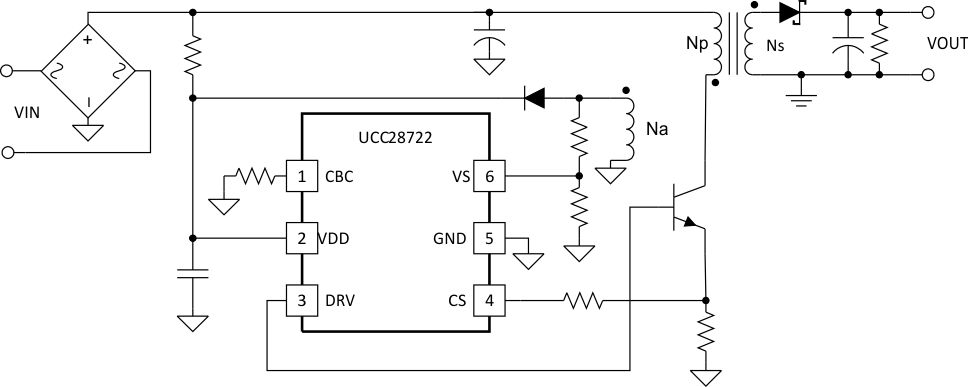
The UCC28722 flyback power supply controller provides isolated-output constant-voltage (CV) and constant-current (CC) output regulation without the use of an optical coupler. The device processes information from the primary power switch and an auxiliary flyback winding for precise control of output voltage and current.
Dynamically-controlled operating states and a tailored modulation profile support high-efficiency operation at all load levels without sacrificing output transient response.
Control algorithms in the UCC28722 device allow operating efficiencies to meet or exceed applicable standards. The output drive interfaces to a bipolar transistor power switch, enabling lower-cost converter design. Discontinuous conduction mode (DCM) with valley switching reduces switching losses, while modulation of switching frequency and primary current peak amplitude (FM and AM) keeps the conversion efficiency high across the entire load and line ranges.
The controller has a maximum switching frequency of 80 kHz and always maintains control of the peak-primary current in the transformer. Output overvoltage and overcurrent as well as input undervoltage protection features help keep primary and secondary component stresses in check. The UCC28722 also allows compensation for voltage drop in the cable to be programmed with an external resistor.
Device Information(1)
| PART NUMBER | PACKAGE | BODY SIZE (NOM) |
|---|---|---|
| UCC28722 | DBV (6) | 2.90 mm × 1.60 mm |
- For all available packages, see the orderable addendum at the end of the data sheet.
