SCDS241B May 2008 – December 2016 TS5A9411
PRODUCTION DATA.
- 1 Features
- 2 Applications
- 3 Description
- 4 Revision History
- 5 Pin Configuration and Functions
- 6 Specifications
- 7 Parameter Measurement Information
- 8 Detailed Description
- 9 Application and Implementation
- 10Power Supply Recommendations
- 11Layout
- 12Device and Documentation Support
- 13Mechanical, Packaging, and Orderable Information
Package Options
Mechanical Data (Package|Pins)
- DCK|6
Thermal pad, mechanical data (Package|Pins)
Orderable Information
1 Features
- Specified Break-Before-Make Switching
- Low ON-State Resistance
(10-Ω Maximum at VCC = 5 V) - Low Power Consumption
- TTL- and CMOS-Compatible Control Input
- Low Input and Output Capacitance
- Excellent ON-State Resistance Matching
- Low Total Harmonic Distortion
- 2.25-V to 5.5-V Single-Supply Operation
- Latch-Up Performance Exceeds 100 mA
Per JESD 78, Class II - ESD Performance Tested Per JESD 22
- 2000-V Human-Body Model
(A114-B, Class II) - 1000-V Charged-Device Model (C101)
- 2000-V Human-Body Model
- Control Inputs Are 5.5-V Tolerant
2 Applications
- Cell Phones
- Communication Systems
- Portable Test Equipment
- Battery Operated Systems
- Sample-and-Hold Circuits
3 Description
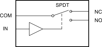
The TS5A9411 device is a bidirectional, single-pole double-throw (SPDT) analog switch that is designed to operate from 2.25 V to 5.5 V. The device offers low ON-state resistance, low leakage, and low power with a break-before-make feature. These features make this device suitable for portable and battery-powered applications.
Device Information(1)
| PART NUMBER | PACKAGE | BODY SIZE (NOM) |
|---|---|---|
| TS5A9411 | SOT (6) | 2.00 mm × 1.25 mm |
- For all available packages, see the orderable addendum at the end of the data sheet.
Simplified Schematic
