SLWS213A January 2010 – November 2015 TRF370417
PRODUCTION DATA.
- 1 Features
- 2 Applications
- 3 Description
- 4 Revision History
- 5 Pin Configuration and Functions
- 6 Specifications
- 7 Detailed Description
- 8 Application and Implementation
- 9 Power Supply Recommendations
- 10Layout
- 11Device and Documentation Support
- 12Mechanical, Packaging, and Orderable Information
Package Options
Mechanical Data (Package|Pins)
- RGE|24
Thermal pad, mechanical data (Package|Pins)
- RGE|24
Orderable Information
1 Features
- 76-dBc Single-Carrier WCDMA ACPR at –8 dBm Channel Power
- Low Noise Floor: –162.3 dBm/Hz at 2140 MHz
- OIP3 of 26.5 dBm at 2140 MHz
- P1dB of 12 dBm at 2140 MHz
- Carrier Feedthrough of –38 dBm at 2140 MHz
- Side-Band Suppression of –50 dBc at 2140 MHz
- Single Supply: 4.5-V–5.5-V Operation
- Silicon Germanium Technology
- 1.7-V CM at I, Q Baseband Inputs
2 Applications
- Cellular Base Station Transceiver
- CDMA: IS95, UMTS, CDMA2000, TD-SCDMA
- TDMA: GSM, IS-136, EDGE/UWC-136
- Multicarrier GSM
- WiMAX: 802.16d/e
- 3GPP: LTE
- Point-to-Point (P2P) Microwave
- Wideband Software-Defined Radio
- Public Safety: TETRA/APC025
- Communication-System Testers
- Cable Modem Termination System (CMTS)
3 Description
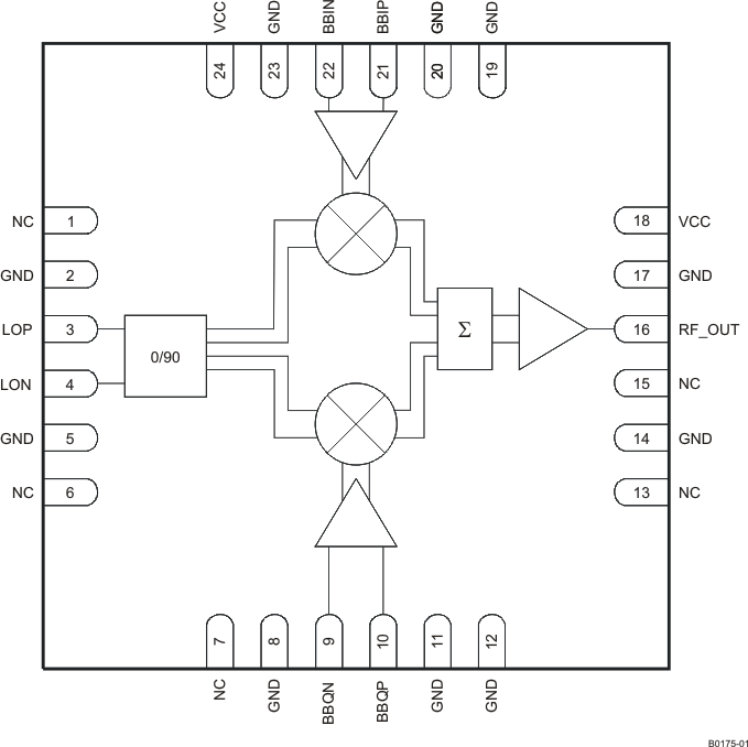
The TRF370417 is a low-noise direct quadrature modulator, capable of converting complex modulated signals from baseband or IF directly up to RF. The TRF370417 is a high-performance, superior-linearity device that operates at RF frequencies of 50 MHz through 6 GHz. The modulator is implemented as a double-balanced mixer. The RF output block consists of a differential to single-ended converter and an RF amplifier capable of driving a single-ended 50-Ω load without any need of external components. The TRF370417 requires a 1.7-V common-mode voltage for optimum linearity performance.
Device Information(1)
| PART NUMBER | PACKAGE | BODY SIZE (NOM) |
|---|---|---|
| TRF370417 | VQFN(24) | 4.00 mm × 4.00 mm |
- For all available packages, see the orderable addendum at the end of the data sheet.
Block Diagram

4 Revision History
Changes from * Revision (January 2010) to A Revision
- Added ESD Ratings table, Feature Description section, Device Functional Modes, Application and Implementation section, Power Supply Recommendations section, Layout section, Device and Documentation Support section, and Mechanical, Packaging, and Orderable Information section.Go