SLVSDD9 March 2017 TPS92692 , TPS92692-Q1
PRODUCTION DATA.
- 1 Features
- 2 Applications
- 3 Description
- 4 Revision History
- 5 Pin Configuration and Functions
- 6 Specifications
-
7 Detailed Description
- 7.1 Overview
- 7.2 Functional Block Diagram
- 7.3
Feature Description
- 7.3.1 Internal Regulator and Undervoltage Lockout (UVLO)
- 7.3.2 Oscillator
- 7.3.3 Spread Spectrum Frequency Modulation
- 7.3.4 Gate Driver
- 7.3.5 Rail-to-Rail Current Sense Amplifier
- 7.3.6 Transconductance Error Amplifier
- 7.3.7 Switch Current Sense
- 7.3.8 Slope Compensation
- 7.3.9 Analog Adjust Input
- 7.3.10 DIM/PWM Input
- 7.3.11 Series P-Channel FET Dimming Gate Driver Output
- 7.3.12 Soft-Start
- 7.3.13 Current Monitor Output
- 7.3.14 Output Overvoltage Protection
- 7.3.15 Output Short-circuit Protection
- 7.3.16 Thermal Protection
- 7.3.17 Fault Indicator (FLT)
- 7.4 Device Functional Modes
-
8 Application and Implementation
- 8.1
Application Information
- 8.1.1 Duty Cycle Considerations
- 8.1.2 Inductor Selection
- 8.1.3 Output Capacitor Selection
- 8.1.4 Input Capacitor Selection
- 8.1.5 Main Power MOSFET Selection
- 8.1.6 Rectifier Diode Selection
- 8.1.7 LED Current Programming
- 8.1.8 Switch Current Sense Resistor
- 8.1.9 Slope Compensation
- 8.1.10 Feedback Compensation
- 8.1.11 Soft-Start
- 8.1.12 Overvoltage and Undervoltage Protection
- 8.1.13 Analog to PWM Dimming Considerations
- 8.1.14 Direct PWM Dimming Considerations
- 8.1.15 Series P-Channel MOSFET Selection
- 8.2
Typical Applications
- 8.2.1
Typical Boost LED Driver
- 8.2.1.1 Design Requirements
- 8.2.1.2
Detailed Design Procedure
- 8.2.1.2.1 Calculating Duty Cycle
- 8.2.1.2.2 Setting Switching Frequency
- 8.2.1.2.3 Setting Dither Modulation Frequency
- 8.2.1.2.4 Inductor Selection
- 8.2.1.2.5 Output Capacitor Selection
- 8.2.1.2.6 Input Capacitor Selection
- 8.2.1.2.7 Main N-Channel MOSFET Selection
- 8.2.1.2.8 Rectifying Diode Selection
- 8.2.1.2.9 Programming LED Current
- 8.2.1.2.10 Setting Switch Current Limit
- 8.2.1.2.11 Programming Slope Compensation
- 8.2.1.2.12 Deriving Compensator Parameters
- 8.2.1.2.13 Setting Start-up Duration
- 8.2.1.2.14 Setting Overvoltage Protection Threshold
- 8.2.1.2.15 Analog-to-PWM Dimming Considerations
- 8.2.1.3 Application Curves
- 8.2.2
Typical Buck-Boost LED Driver
- 8.2.2.1 Design Requirements
- 8.2.2.2
Detailed Design Procedure
- 8.2.2.2.1 Calculating Duty Cycle
- 8.2.2.2.2 Setting Switching Frequency
- 8.2.2.2.3 Setting Dither Modulation Frequency
- 8.2.2.2.4 Inductor Selection
- 8.2.2.2.5 Output Capacitor Selection
- 8.2.2.2.6 Input Capacitor Selection
- 8.2.2.2.7 Main N-Channel MOSFET Selection
- 8.2.2.2.8 Rectifier Diode Selection
- 8.2.2.2.9 Programming LED Current
- 8.2.2.2.10 Setting Switch Current Limit and Slope Compensation
- 8.2.2.2.11 Programming Slope Compensation
- 8.2.2.2.12 Deriving Compensator Parameters
- 8.2.2.2.13 Setting Startup Duration
- 8.2.2.2.14 Setting Overvoltage Protection Threshold
- 8.2.2.2.15 Direct PWM Dimming Consideration
- 8.2.2.3 Application Curves
- 8.2.1
Typical Boost LED Driver
- 8.1
Application Information
- 9 Power Supply Recommendations
- 10Layout
- 11Device and Documentation Support
- 12Mechanical, Packaging, and Orderable Information
Package Options
Mechanical Data (Package|Pins)
- PWP|20
Thermal pad, mechanical data (Package|Pins)
- PWP|20
Orderable Information
1 Features
- Wide Input Voltage: 4.5 V to 65 V
- Better than ± 4% LED Current Accuracy over –40°C to 150°C Junction Temperature Range
- Spread Spectrum Frequency Modulation for Improved EMI
- Comprehensive Fault Protection Circuitry with Current Monitor output and Open Drain Fault Flag Indicator
- Internal Analog Voltage to PWM Duty Cycle Generator for stand-alone Dimming Operation
- Compatible with Direct PWM Input with over 1000:1 Dimming Range
- Analog LED Current Adjust Input (IADJ) with over 15:1 Contrast Ratio
- Integrated P-Channel Driver to enable Series FET Dimming and LED Protection
- TPS92692-Q1: Automotive Q100 Grade 1 Qualified
2 Applications
- TPS92692-Q1: Automotive Exterior Lighting Applications
- Driver Monitoring Systems (DMS)
- LED General Lighting Applications
- Exit Signs and Emergency Lighting
3 Description
The TPS92692 and TPS92692-Q1 are high accuracy peak current mode based controllers designed to support step-up/down LED driver topologies. The device incorporates a rail-to-rail current amplifier to measure LED current and spread spectrum frequency modulation technique for improved EMI performance.
This high performance LED controller can independently modulate LED current using either analog or PWM dimming techniques. Linear analog dimming response with over 15:1 range is obtained by varying the voltage across the high impedance analog adjust (IADJ) input. PWM dimming of LED current is achieved by directly modulating the DIM/PWM input pin with the desired duty cycle or by enabling the internal PWM generator circuit. The PWM generator translates the DC voltage at DIM/PWM pin to corresponding duty cycle by comparing it to the internal triangle wave generator. The optional PDRV gate driver output can be used to drive an external P-Channel series MOSFET.
The TPS92692 and TPS92692-Q1 devices support continuous LED status check through the current monitor (IMON) output. The devices also include an open drain fault indicator output to indicate LED overcurrent, output overvoltage and output undervoltage conditions.
Device Information(1)
| PART NUMBER | PACKAGE | BODY SIZE (NOM) |
|---|---|---|
| TPS92692-Q1 | HTSSOP (20) | 5.10 mm × 6.60 mm |
| TPS92692 |
- For all available packages, see the orderable addendum at the end of the data sheet.
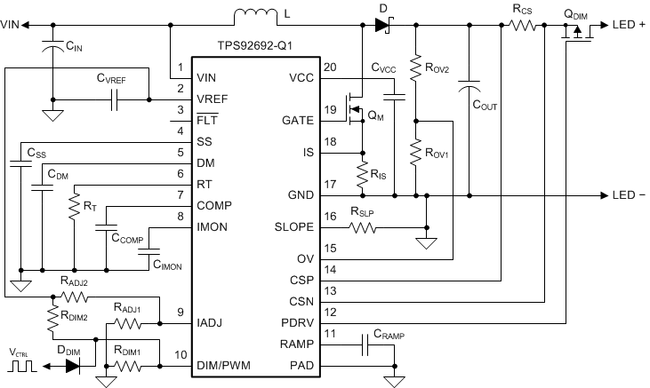
Typical Boost LED Driver

4 Revision History
| DATE | REVISION | NOTES |
|---|---|---|
| March 2017 | * | Initial release. |