SLVSD68 December 2015 TPS92691 , TPS92691-Q1
PRODUCTION DATA.
- 1 Features
- 2 Applications
- 3 Description
- 4 Revision History
- 5 Pin Configuration and Functions
- 6 Specifications
-
7 Detailed Description
- 7.1 Overview
- 7.2 Functional Block Diagram
- 7.3
Feature Description
- 7.3.1 Internal Regulator and Undervoltage Lockout (UVLO)
- 7.3.2 Oscillator
- 7.3.3 Gate Driver
- 7.3.4 Rail-to-Rail Current Sense Amplifier
- 7.3.5 Transconductance Error Amplifier
- 7.3.6 Switch Current Sense and Internal Slope Compensation
- 7.3.7 Analog Adjust Input
- 7.3.8 PWM Input and Series Dimming FET Gate Driver Output
- 7.3.9 Soft-Start
- 7.3.10 Current Monitor Output
- 7.3.11 Overvoltage Protection
- 7.3.12 Thermal Protection
- 7.4 Device Functional Modes
-
8 Application and Implementation
- 8.1
Application Information
- 8.1.1 Duty Cycle Considerations
- 8.1.2 Inductor Selection
- 8.1.3 Output Capacitor Selection
- 8.1.4 Input Capacitor Selection
- 8.1.5 Main Power MOSFET Selection
- 8.1.6 Rectifier Diode Selection
- 8.1.7 LED Current Programming
- 8.1.8 Switch Current Sense Resistor and Slope Compensation
- 8.1.9 Feedback Compensation
- 8.1.10 Soft-Start
- 8.1.11 Overvoltage Protection
- 8.1.12 PWM Dimming Considerations
- 8.2
Typical Applications
- 8.2.1
Typical Boost LED Driver
- 8.2.1.1 Design Requirements
- 8.2.1.2
Detailed Design Procedure
- 8.2.1.2.1 Calculating Duty Cycle
- 8.2.1.2.2 Setting Switching Frequency
- 8.2.1.2.3 Inductor Selection
- 8.2.1.2.4 Output Capacitor Selection
- 8.2.1.2.5 Input Capacitor Selection
- 8.2.1.2.6 Main N-Channel MOSFET Selection
- 8.2.1.2.7 Rectifying Diode Selection
- 8.2.1.2.8 Programming LED Current
- 8.2.1.2.9 Setting Switch Current Limit and Slope Compensation
- 8.2.1.2.10 Deriving Compensator Parameters
- 8.2.1.2.11 Setting Start-up Duration
- 8.2.1.2.12 Setting Overvoltage Protection Threshold
- 8.2.1.2.13 PWM Dimming Considerations
- 8.2.1.3 Application Curves
- 8.2.2
Typical Buck-Boost LED Driver
- 8.2.2.1 Design Requirements
- 8.2.2.2
Detailed Design Procedure
- 8.2.2.2.1 Calculating Duty Cycle
- 8.2.2.2.2 Setting Switching Frequency
- 8.2.2.2.3 Inductor Selection
- 8.2.2.2.4 Output Capacitor Selection
- 8.2.2.2.5 Input Capacitor Selection
- 8.2.2.2.6 Main N-Channel MOSFET Selection
- 8.2.2.2.7 Rectifier Diode Selection
- 8.2.2.2.8 Setting Switch Current Limit and Slope Compensation
- 8.2.2.2.9 Programming LED Current
- 8.2.2.2.10 Deriving Compensator Parameters
- 8.2.2.2.11 Setting Startup Duration
- 8.2.2.2.12 Setting Overvoltage Protection Threshold
- 8.2.2.2.13 PWM Dimming Consideration
- 8.2.2.3 Application Curves
- 8.2.1
Typical Boost LED Driver
- 8.1
Application Information
- 9 Power Supply Recommendations
- 10Layout
- 11Device and Documentation Support
- 12Mechanical, Packaging, and Orderable Information
Package Options
Mechanical Data (Package|Pins)
- PWP|16
Thermal pad, mechanical data (Package|Pins)
- PWP|16
Orderable Information
1 Features
- Wide Input Voltage: 4.5 V to 65 V
- Wide Output Voltage Range: 2 V to 65 V
- Low Input Offset Rail-to-Rail Current Sense Amplifier
- Better than ±3% LED Current Accuracy over 25°C to 140°C Junction Temperature Range
- Compatible With High-Side and Low-Side Current Sense Implementations
- High-Impedance Analog LED Current Adjust Input (IADJ) With over 15:1 Contrast Ratio
- Over 1000:1 Series FET PWM Dimming Ratio With Integrated Series N-Channel Dim Driver Interface
- Continuous LED Current Monitor Output for System Fault Detection and Diagnoses
- Programmable Switching Frequency With External Clock Synchronization Capability
- Programmable Soft-Start and Slope Compensation
- Comprehensive Fault Protection Circuitry Including VCC Undervoltage Lockout (UVLO), Output Overvoltage Protection (OVP), Cycle-by-Cycle Switch Current Limit, and Thermal Protection
- TPS92691-Q1: Automotive Q100 Grade 1 Qualified
2 Applications
- TPS92691-Q1: Automotive Exterior Lighting Applications
- Architectural and General Lighting Applications
3 Description
The TPS92691/-Q1 is a versatile LED controller that can support a range of step-up or step-down driver topologies. The device implements a fixed-frequency peak current mode control technique with programmable switching frequency, slope compensation, and soft-start timing. It incorporates a high voltage (65-V) rail-to-rail current sense amplifier that can directly measure LED current using either a high-side or a low-side series sense resistor. The amplifier is designed to achieve low input offset voltage and attain better than ±3% LED current accuracy over junction temperature range of 25°C to 140°C and output common-mode voltage range of 0 to 60 V.
LED current can be independently modulated using either analog or PWM dimming techniques. Linear analog dimming response with 15:1 range is obtained by varying the voltage from 140 mV to 2.25 V across the high impedance analog adjust (IADJ) input. PWM dimming of LED current is achieved by modulating the PWM input pin with the desired duty cycle and frequency. Optional DDRV gate driver output can be used to enable series FET dimming functionality to get over 1000:1 contrast ratio.
The TPS92691/-Q1 supports continuous LED status check through the current monitor (IMON) output. This allows for LED short circuit or open circuit detection and protection. Additional fault protection features include VCC UVLO, output OVP, switch cycle-by-cycle current limit, and thermal protection.
Device Information(1)
| PART NUMBER | PACKAGE | BODY SIZE (NOM) |
|---|---|---|
| TPS92691-Q1 TPS92691 |
HTSSOP (16) | 5.10 mm × 6.60 mm |
- For all available packages, see the orderable addendum at the end of the data sheet.
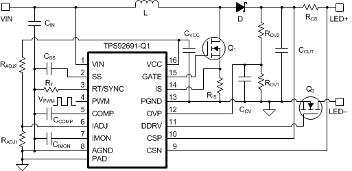
Typical Boost LED Driver Application Schematic

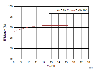
Efficiency vs Output Voltage
