SNVSBL0A November 2020 – December 2021 TPS7H4010-SEP
PRODUCTION DATA
- 1 Features
- 2 Applications
- 3 Description
- 4 Revision History
- 5 Pin Configuration and Functions
- 6 Specifications
-
7 Detailed Description
- 7.1 Overview
- 7.2 Functional Block Diagram
- 7.3
Feature Description
- 7.3.1 Synchronous Step-Down Regulator
- 7.3.2 Auto Mode and FPWM Mode
- 7.3.3 Fixed-Frequency Peak Current-Mode Control
- 7.3.4 Adjustable Output Voltage
- 7.3.5 Enable and UVLO
- 7.3.6 Internal LDO, VCC_UVLO, and BIAS Input
- 7.3.7 Soft Start and Voltage Tracking
- 7.3.8 Adjustable Switching Frequency
- 7.3.9 Frequency Synchronization and Mode Setting
- 7.3.10 Internal Compensation and CFF
- 7.3.11 Bootstrap Capacitor and VBOOT-UVLO
- 7.3.12 Power-Good and Overvoltage Protection
- 7.3.13 Overcurrent and Short-Circuit Protection
- 7.3.14 Thermal Shutdown
- 7.4 Device Functional Modes
-
8 Application and Implementation
- 8.1 Application Information
- 8.2
Typical Application
- 8.2.1 Design Requirements
- 8.2.2
Detailed Design Procedure
- 8.2.2.1 Output Voltage Setpoint
- 8.2.2.2 Switching Frequency
- 8.2.2.3 Input Capacitors
- 8.2.2.4 Inductor Selection
- 8.2.2.5 Output Capacitor Selection
- 8.2.2.6 Feed-Forward Capacitor
- 8.2.2.7 Bootstrap Capacitors
- 8.2.2.8 VCC Capacitor
- 8.2.2.9 BIAS
- 8.2.2.10 Soft Start
- 8.2.2.11 Undervoltage Lockout Setpoint
- 8.2.2.12 PGOOD
- 8.2.3 Application Curves
- 9 Power Supply Recommendations
- 10Layout
- 11Device and Documentation Support
- 12Mechanical, Packaging, and Orderable Information
Package Options
Refer to the PDF data sheet for device specific package drawings
Mechanical Data (Package|Pins)
- RNP|30
- KGD|0
Thermal pad, mechanical data (Package|Pins)
- RNP|30
Orderable Information
1 Features
- Radiation Hardened
- SEL, SEB, and SEGR immune up to
LET = 43 MeV-cm2/mg - SET and SEFI
characterized up to
LET = 43 MeV-cm2/mg - TID assured for every wafer lot up to
20 krad(Si) - TID characterized up to 30 krad(Si)
- SEL, SEB, and SEGR immune up to
- Space Enhanced Plastic
- Controlled baseline
- Au bondwire and NiPdAu lead finish
- Enhanced mold compound for low outgassing
- One fabrication, assembly and test site
- Extended product life cycle
- Extended product change notification
- Product traceability
- Wide voltage conversion range:
- tON-MIN = 60 ns (typical)
- tOFF-MIN = 70 ns (typical)
- Low MOSFET ON-resistance:
- RDS_ON_HS = 53 mΩ (typical)
- RDS_ON_LS = 31 mΩ (typical)
- Adjustable frequency range: 350 kHz to 2.2 MHz
- Synchronizable to external clock
- Internal compensation
- Power-good flag
- Precision enable to program system UVLO
- Fixed or adjustable soft-start time
- Cycle-by-cycle current limiting
- Short-circuit protection with hiccup mode
- Thermal shutdown protection
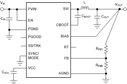
 Simplified Schematic