SBVS263A July 2017 – September 2017 TPS7A39
PRODUCTION DATA.
- 1 Features
- 2 Applications
- 3 Description
- 4 Revision History
- 5 Pin Configuration and Functions
- 6 Specifications
- 7 Detailed Description
-
8 Application and Implementation
- 8.1
Application Information
- 8.1.1 Setting the Output Voltages on Adjustable Devices
- 8.1.2 Capacitor Recommendations
- 8.1.3 Input and Output Capacitor (CINx and COUTx)
- 8.1.4 Feed-Forward Capacitor (CFFx)
- 8.1.5 Noise-Reduction and Soft-Start Capacitor (CNR/SS)
- 8.1.6 Buffered Reference Voltage
- 8.1.7 Overriding Internal Reference
- 8.1.8 Start-Up
- 8.1.9 AC and Transient Performance
- 8.1.10 DC Performance
- 8.1.11 Reverse Current
- 8.1.12 Power Dissipation (PD)
- 8.2 Typical Applications
- 8.1
Application Information
- 9 Power-Supply Recommendations
- 10Layout
- 11Device and Documentation Support
- 12Mechanical, Packaging, and Orderable Information
Package Options
Mechanical Data (Package|Pins)
- DSC|10
Thermal pad, mechanical data (Package|Pins)
- DSC|10
Orderable Information
1 Features
- Positive and Negative LDOs in One Package
- Wide Input Voltage Range: ±3.3 V to ±33 V
- Wide Output Voltage Range:
- Positive Range: 1.2 V to 30 V
- Negative Range: –30 V to 0 V
- Output Current: 150 mA per Channel
- Monotonic Start-Up Tracking
- High Power-Supply Rejection Ratio (PSRR):
- 69 dB (120 Hz)
- ≥ 50 dB (10 Hz to 2 MHz)
- Output Voltage Noise: 21 µVRMS (10 Hz–100 kHz)
- Buffered 1.2-V Reference Output
- Stable With a 10-µF or Larger Output Capacitor
- Single Positive-Logic Enable
- Adjustable Soft-Start In-Rush Control
- 3-mm × 3-mm, 10-Pin WSON Package
- Low Thermal Resistance: RθJA = 44.4°C/W
- Operating Temperature Range: –40 to +125°C
2 Applications
- Supply Rails for Op Amps, ADCs, DACs, and Other High-Precision Analog Circuitry
- Post DC-DC Regulation and Filtering
- Analog I/O Modules
- Test and Measurement
- Rx, Tx, and PA Circuitry
- Industrial Instrumentation
- Medical Imaging
3 Description
The TPS7A39 device is a dual, monolithic, high-PSRR, positive and negative low-dropout (LDO) voltage regulator capable of sourcing (and sinking) up to 150 mA of current. The regulated outputs can be independently and externally adjusted to symmetrical or asymmetrical voltages, making this device an ideal dual, bipolar power supply for signal conditioning.
Both positive and negative outputs of the TPS7A39 ratiometrically track each other during startup to mitigate floating conditions and other power-supply sequencing issues common in dual-rail systems. The negative output can regulate up to 0 V, extending the common-mode range for single-supply amplifiers. The TPS7A39 also features high PSRR to eliminate power-supply noise, such as switching noise, that can compromise signal integrity.
Both regulators are controlled with a single positive logic enable pin for interfacing with standard digital logic. A capacitor-programmable soft-start function controls in-rush current and start-up time. The internal reference voltage of the TPS7A39 can be overridden with an external reference to enable precision outputs, output voltage margining, or to track other power supplies. Additionally, the TPS7A39 has a buffered reference output that can be used as a voltage reference for other components in the system.
These features make the TPS7A39 a robust, simplified solution to power operational amplifiers, digital-to-analog converters (DACs), and other precision analog circuitry.
Device Information(1)
| PART NUMBER | PACKAGE | BODY SIZE (NOM) |
|---|---|---|
| TPS7A39 | WSON (10) | 3.00 mm × 3.00 mm |
- For all available packages, see the orderable addendum at the end of the data sheet.
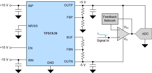
Powering the Signal Chain

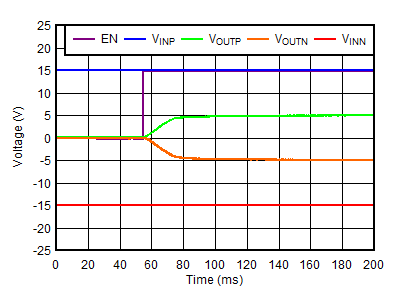
Monotonic Start-Up Tracking
