SLVSC85C August 2013 – May 2015 TPS65279
PRODUCTION DATA.
- 1 Features
- 2 Applications
- 3 Description
- 4 Revision History
- 5 Description (continued)
- 6 Pin Configuration and Functions
- 7 Specifications
-
8 Detailed Description
- 8.1 Overview
- 8.2 Functional Block Diagram
- 8.3
Feature Description
- 8.3.1 Enable and Adjusting Undervoltage Lockout (UVLO)
- 8.3.2 Adjustable Switching Frequency and Synchronization
- 8.3.3 Soft-Start Time
- 8.3.4 Out-of-Phase Operation
- 8.3.5 Output Overvoltage Protection (OVP)
- 8.3.6 Bootstrap Voltage (BOOT) and Low Dropout Operation
- 8.3.7 Overcurrent Protection
- 8.3.8 Current Sharing Operation
- 8.3.9 Thermal Shutdown
- 8.4 Device Functional Modes
- 9 Application and Implementation
- 10Power Supply Recommendations
- 11Layout
- 12Device and Documentation Support
- 13Mechanical, Packaging, and Orderable Information
Package Options
Mechanical Data (Package|Pins)
Thermal pad, mechanical data (Package|Pins)
Orderable Information
1 Features
- 4.5-V to 18-V Wide Input Voltage Range
- Programmable Slew Rate Control for Output Voltage Transition
- Up to 5-A Maximum Continuous Output Current in Buck 1 and Buck 2
- Buck 1 and Buck 2 can be Paralleled to Deliver up to 10-A Current
- Pulse Skipping Mode to Achieve High Efficiency in Light Load
- Adjustable Switching Frequency
200 kHz to 1.6 MHz Set by External Resistor - Dedicated Enable and Soft-Start for Each Buck
- Peak Current-Mode Control With Simple Compensation Circuit
- Cycle-by-Cycle Overcurrent Protection
- 180° Out-of-Phase Operation to Reduce Input Capacitance and Power Supply Induced Noise
- Over Temperature Protection
- Available in 32-Pin Thermally Enhanced HTSSOP (DAP) and 36-Pin VQFN 6-mm × 6-mm (RHH) Packages
3 Description
TPS65279 is a monolithic dual synchronous buck converter with wide 4.5-V to 18-V operating input voltage range that encompassed most intermediate bus voltage operating off 5-, 9-, 12- or 15-V power bus or battery. The converter with constant frequency peak current mode control is designed to simplify its application while giving the designers options to optimize their usage according to the target applications.
Two bucks in TPS65279 can be paralleled to delivery up to 10-A load current by using current sharing mode, connect ISHARE pin high. Two phase operation in current sharing reduces system filtering capacitance and inductance, alleviates EMI and improves output voltage ripple and noise.
TPS65279 features a dedicated enable pin. An independent soft-start pin provides flexibility in power up programmability. Constant frequency peak current mode control simplifies the compensation and provides fast transient response. Cycle-by-cycle overcurrent protection and hiccup mode operation limit MOSFET power dissipation in short circuit or over loading fault conditions.
Device Information(1)
| PART NUMBER | PACKAGE | BODY SIZE (NOM) |
|---|---|---|
| TPS65279 | HTSSOP (32) | 6.20 mm × 11.00 mm |
| VQFN (36) | 6.00 mm × 6.00 mm |
- For all available packages, see the orderable addendum at the end of the data sheet.
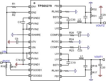
Typical Application Schematic

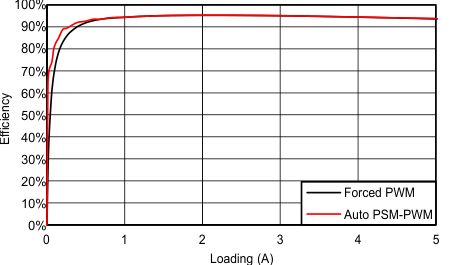
Efficiency vs Loading
