SLVS849C July 2008 – September 2017 TPS65100-Q1
PRODUCTION DATA.
- 1 Features
- 2 Applications
- 3 Description
- 4 Revision History
- 5 Pin Configuration and Functions
- 6 Specifications
- 7 Detailed Description
-
8 Application and Implementation
- 8.1 Application Information
- 8.2
Typical Applications
- 8.2.1
Supply for a Typical Approximately 7-inch Display
- 8.2.1.1 Design Requirements
- 8.2.1.2
Detailed Design Procedure
- 8.2.1.2.1
Boost Converter Design Procedure
- 8.2.1.2.1.1 Inductor Selection
- 8.2.1.2.1.2 Output Capacitor Selection
- 8.2.1.2.1.3 Input Capacitor Selection
- 8.2.1.2.1.4 Rectifier Diode Selection
- 8.2.1.2.1.5 Converter Loop Design and Stability
- 8.2.1.2.1.6 Design Procedure Quick Steps
- 8.2.1.2.1.7 Setting the Output Voltage and Selecting the Feedforward Capacitor
- 8.2.1.2.2 Negative Charge Pump
- 8.2.1.2.3 Positive Charge Pump
- 8.2.1.2.4 VCOM Buffer
- 8.2.1.2.5 Linear Regulator Controller
- 8.2.1.2.1
Boost Converter Design Procedure
- 8.2.1.3 Application Curves
- 8.2.2 Supply for a Typical Approximately 8-inch Display
- 8.2.1
Supply for a Typical Approximately 7-inch Display
- 9 Power Supply Recommendations
- 10Layout
- 11Device and Documentation Support
- 12Mechanical, Packaging, and Orderable Information
Package Options
Mechanical Data (Package|Pins)
- PWP|24
Thermal pad, mechanical data (Package|Pins)
- PWP|24
Orderable Information
1 Features
- Qualified for Automotive Applications
- AEC-Q100 Qualified With the Following Results:
- Device Temperature Grade 1: –40°C to 125°C Ambient Operating Temperature Range
- Device HBM ESD Classification Level 2
- Device CDM ESD Classification Level C5
- Input Voltage Range: 2.7-V to 5.8-V
- VO1 Boost Converter
- Up to 15 V Output Voltage
- Virtual Synchronous Converter Topology
- < 1% Output Voltage Accuracy
- 1.6-MHz Fixed Switching Frequency
- 2.3-A Switch Current Limit
- VO2 Negative Regulated Charge Pump
- Down to -12 V / 20 mA
- VO3 Positive Regulated Charge Pump
- Up to 30 V / 20 mA
- Three Independently Adjustable Outputs
- Integrated VCOM Buffer
- Auxiliary 3.3-V Linear Regulator Controller
- Internal Soft Start
- Internal Power-On Sequencing
- Protection Features
- Short-Circuit Detection of all Outputs
- Overvoltage Protection of all Outputs
- Thermal Shutdown
- Available in TSSOP-24 PowerPAD™ Package
2 Applications
- Infotainment Systems
- Automotive Displays
- Instrument Clusters
- Center Consoles
- Rear Seat Entertainment
3 Description
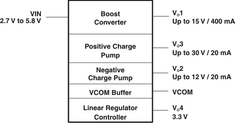
The TPS65100-Q1 device offers a compact and small power supply solution that provides all three voltages required by thin-film transistor (TFT) LCD displays. The auxiliary linear regulator controller can be used to generate a 3.3-V logic power rail for systems powered by a 5-V supply rail only.
The main output, VO1, is a 1.6-MHz fixed-frequency PWM boost converter that provides the source-drive voltage for the LCD display. The TPS65100-Q1 has a typical switch current limit of 2.3 A. A fully integrated adjustable charge pump doubler-tripler provides the positive LCD gate-drive voltage. An externally adjustable negative charge pump provides the negative gate-drive voltage.
The TPS65100-Q1 has an integrated VCOM buffer to power the LCD backplane. For LCD panels powered by 5 V only, the TPS65100-Q1 device has a linear regulator controller using an external transistor to provide a regulated 3.3-V output for the digital circuits. For maximum safety, the TPS65100-Q1 device goes into shutdown as soon as one of the outputs is out of regulation. The device can be enabled again by toggling the input or the enable (EN) pin to GND.
Device Information(1)
| PART NUMBER | PACKAGE | BODY SIZE (NOM) |
|---|---|---|
| TPS65100-Q1 | TSSOP (24) with PowerPAD | 4.40 mm × 7.80 mm |
- For all available packages, see the orderable addendum at the end of the data sheet.
TPS65100-Q1 Overview
