SLVS774C June 2007 – January 2016 TPS650240 , TPS650241 , TPS650242 , TPS650243 , TPS650244 , TPS650245
PRODUCTION DATA.
- 1 Features
- 2 Applications
- 3 Description
- 4 Revision History
- 5 Description (continued)
- 6 Pin Configuration and Functions
-
7 Specifications
- 7.1 Absolute Maximum Ratings
- 7.2 ESD Ratings
- 7.3 Recommended Operating Conditions
- 7.4 Thermal Information
- 7.5 Electrical Characteristics: Control Signals and Supply Pins
- 7.6 Electrical Characteristics: VDCDC1 Step-Down Converter
- 7.7 Electrical Characteristics: VDCDC2 Step-Down Converter
- 7.8 Electrical Characteristics: VDCDC3 Step-Down Converter
- 7.9 Electrical Characteristics: General
- 7.10 Typical Characteristics
- 8 Detailed Description
- 9 Application and Implementation
- 10Power Supply Recommendations
- 11Layout
- 12Device and Documentation Support
- 13Mechanical, Packaging, and Orderable Information
Package Options
Mechanical Data (Package|Pins)
- RHB|32
Thermal pad, mechanical data (Package|Pins)
- RHB|32
Orderable Information
1 Features
- 1.6-A, 1.0-A, or 0.8-A, 97% Efficient Step-Down Converter for System Voltage (VDCDC1)
- 3.3 V or 2.80 V or Adjustable
- 1.6-A, 1.0-A, or 0.8-A, up to 95% Efficient Step-Down Converter for Memory Voltage (VDCDC2)
- 1.8 V or 2.5 V or Adjustable
- 0.8-A, 90% Efficient Step-Down Converter for Processor Core (VDCDC3)
- Two Selectable Voltages for VDCDC3
- TPS650240:
- DEFDCDC3 = LOW: VO = 1.0 V
- DEFDCDC3 = HIGH: VO = 1.3 V
- TPS650241:
- DEFDCDC3 = LOW: VO = 0.9 V
- DEFDCDC3 = HIGH: VO= 1.375 V
- TPS650242:
- DEFDCDC3 = LOW: VO = 1.0 V
- DEFDCDC3 = HIGH: VO = 1.5 V
- TPS650243:
- DEFDCDC3 = LOW: VO = 1.0 V
- DEFDCDC3 = HIGH: VO = 1.2 V
- TPS650244:
- DEFDCDC3 = LOW: VO = 1.55 V
- DEFDCDC3 = HIGH: VO = 1.6 V
- TPS650245:
- DEFDCDC3 = LOW: VO = 0.9 V
- DEFDCDC3 = HIGH: VO = 1.1 V
- TPS650240:
- 30-mA LDO for Vdd_alive
- 2 × 200-mA General-Purpose LDOs (LDO1 and LDO2)
- Dynamic Voltage Management for Processor Core
- LDO1 and LDO2 Voltage Externally Adjustable
- Separate Enable Pins for Inductive Converters
- 2.25-MHz Switching Frequency
- 85-μA Quiescent Current
- Thermal Shutdown Protection
2 Applications
- Split-Supply DSP and μP Solutions, ARM-Based Processors, and so on
- Cellular and Smart Phones
- GPS
- Digital Cameras
- PDA
3 Description
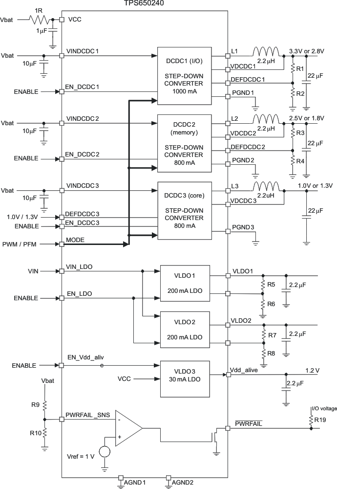
The TPS65024x devices are integrated power management ICs for applications powered by one Li-Ion or Li-Polymer cell, which require multiple power rails. The TPS65024x provide three highly efficient, step-down converters targeted at providing the core voltage, peripheral, I/O, and memory rails in a processor-based system. All three step-down converters enter a low power mode at light load for maximum efficiency across the widest possible range of load currents. The converters can be forced into fixed-frequency PWM mode by pulling the MODE pin high.
Device Information(1)
| PART NUMBER | PACKAGE | BODY SIZE (NOM) |
|---|---|---|
| TPS65024x | VQFN (32) | 5.00 mm × 5.00 mm |
- For all available packages, see the orderable addendum at the end of the data sheet.
Functional Block Diagram

4 Revision History
Changes from B Revision (July 2009) to C Revision
- Added ESD Ratings table, Feature Description section, Device Functional Modes, Application and Implementation section, Power Supply Recommendations section, Layout section, Device and Documentation Support section, and Mechanical, Packaging, and Orderable Information sectionGo
Changes from A Revision (December 2007) to B Revision