SLVSB35C October 2012 – July 2015 TPS62175 , TPS62177
PRODUCTION DATA.
- 1 Features
- 2 Applications
- 3 Description
- 4 Revision History
- 5 Device Comparison Table
- 6 Pin Configuration and Functions
- 7 Specifications
- 8 Detailed Description
-
9 Application and Implementation
- 9.1 Application Information
- 9.2 Typical Application
- 9.3 System Examples
- 10Power Supply Recommendations
- 11Layout
- 12Device and Documentation Support
- 13Mechanical, Packaging, and Orderable Information
Package Options
Refer to the PDF data sheet for device specific package drawings
Mechanical Data (Package|Pins)
- DQC|10
Thermal pad, mechanical data (Package|Pins)
Orderable Information
1 Features
- DCS-Control™ Topology
- Input Voltage Range 4.75 V to 28 V
- Quiescent Current Typically 4.8 µA (Sleep Mode)
- 100% Duty Cycle Mode
- Active Output Discharge
- Power Good Output
- Output Current of 500 mA
- Output Voltage Range 1 VDC to 6 V
- Switching Frequency of Typically 1 MHz
- Seamless Power Save Mode Transition
- Undervoltage Lockout
- Short Circuit Protection
- Over Temperature Protection
- Available in 2-mm × 3-mm 10-pin WSON Package
2 Applications
- General 12 V / 24 V Point Of Load Supply
- Ultra Mobile PC, Embedded PC
- Low Power Supply for Microprocessor
- High Efficiency LDO Alternative
- Industrial Sensors
3 Description
The TPS6217x is a high efficiency synchronous step-down DC/DC converter, based on the DCS-Control™ topology.
With a wide operating input voltage range of 4.75 V to 28 V, the device is ideally suited for systems powered from multi cell Li-Ion as well as 12 V and even higher intermediate supply rails, providing up to 500-mA output current.
The TPS6217x automatically enters power save mode at light loads, to maintain high efficiency across the whole load range. As well, it features a sleep mode to supply applications with advanced power save modes like ultra low power micro controllers. The power good output may be used for power sequencing and/or power on reset.
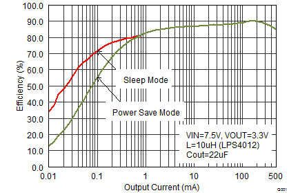
The device features a typical quiescent current of 22 µA in normal mode and 4.8 µA in sleep mode. In sleep mode, the efficiency at very low load currents can be increased by as much as 20%. In shutdown mode, the shutdown current is less than 2 µA and the output is actively discharged.
The TPS6217x, available in an adjustable and a fixed output voltage version, is packaged in a small 2-mm × 3-mm 10-pin WSON package.
Device Information(1)
| PART NUMBER | PACKAGE | BODY SIZE (NOM) |
|---|---|---|
| TPS6217x | WSON (10) | 2.00 mm × 3.00 mm |
- For all available packages, see the orderable addendum at the end of the data sheet.
spacing
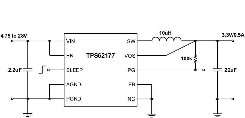
Typical Application Schematic

Efficiency vs Output Current
