SLVS859B June   2008  – December 2014 TPS61085

PRODUCTION DATA.  

  1. Features
  2. Applications
  3. Description
  4. Simplified Schematic
  5. Revision History
  6. Pin Configuration and Functions
  7. Specifications
    1. 7.1 Absolute Maximum Ratings
    2. 7.2 ESD Ratings
    3. 7.3 Recommended Operating Conditions
    4. 7.4 Thermal Information
    5. 7.5 Electrical Characteristics
    6. 7.6 Typical Characteristics
  8. Detailed Description
    1. 8.1 Overview
    2. 8.2 Functional Block Diagram
    3. 8.3 Feature Description
      1. 8.3.1 Soft-Start
      2. 8.3.2 Frequency Select Pin (FREQ)
      3. 8.3.3 Undervoltage Lockout (UVLO)
      4. 8.3.4 Thermal Shutdown
      5. 8.3.5 Overvoltage Prevention
    4. 8.4 Device Functional Modes
  9. Application and Implementation
    1. 9.1 Application Information
    2. 9.2 Typical Application
      1. 9.2.1 Design Requirements
      2. 9.2.2 Detailed Design Procedure
        1. 9.2.2.1 Design Procedure
        2. 9.2.2.2 Inductor Selection
        3. 9.2.2.3 Rectifier Diode Selection
        4. 9.2.2.4 Setting the Output Voltage
        5. 9.2.2.5 Compensation (COMP)
        6. 9.2.2.6 Input Capacitor Selection
        7. 9.2.2.7 Output Capacitor Selection
      3. 9.2.3 Application Curves
    3. 9.3 System Examples
      1. 9.3.1 General Boost Application Circuits
      2. 9.3.2 TFT LCD Application Circuit
      3. 9.3.3 WHITE LED Application Circuits
  10. 10Power Supply Recommendations
  11. 11Layout
    1. 11.1 Layout Guidelines
    2. 11.2 Layout Example
  12. 12Device and Documentation Support
    1. 12.1 Trademarks
    2. 12.2 Electrostatic Discharge Caution
    3. 12.3 Glossary
  13. 13Mechanical, Packaging, and Orderable Information

Package Options

Mechanical Data (Package|Pins)
Thermal pad, mechanical data (Package|Pins)
Orderable Information

1 Features

  • 2.3 V to 6 V Input Voltage Range
  • 18.5-V Boost Converter With 2.0-A Switch Current
  • 650-kHz/1.2-MHz Selectable Switching Frequency
  • Adjustable Soft-Start
  • Thermal Shutdown
  • Undervoltage Lockout
  • 8-Pin VSSOP Package
  • 8-Pin TSSOP Package

2 Applications

  • Handheld Devices
  • GPS Receivers
  • Digital Still Cameras
  • Portable Applications
  • DSL Modems
  • PCMCIA Cards
  • TFT LCD Bias Supply

3 Description

The TPS61085 is a high frequency, high efficiency DC-DC converter with an integrated 2.0-A, 0.13-Ω power switch capable of providing an output voltage up to 18.5 V. The selectable frequency of 650 kHz or 1.2 MHz allows the use of small external inductors and capacitors and provides fast transient response. The external compensation allows optimizing the application for specific conditions. A capacitor connected to the soft-start pin minimizes inrush current at startup.

Device Information(1)

PART NUMBER PACKAGE BODY SIZE (NOM)
TPS61085 VSSOP (8) 3.00 mm × 3.00 mm
TSSOP (8) 3.00 mm × 4.40 mm
  1. For all available packages, see the orderable addendum at the end of the datasheet.
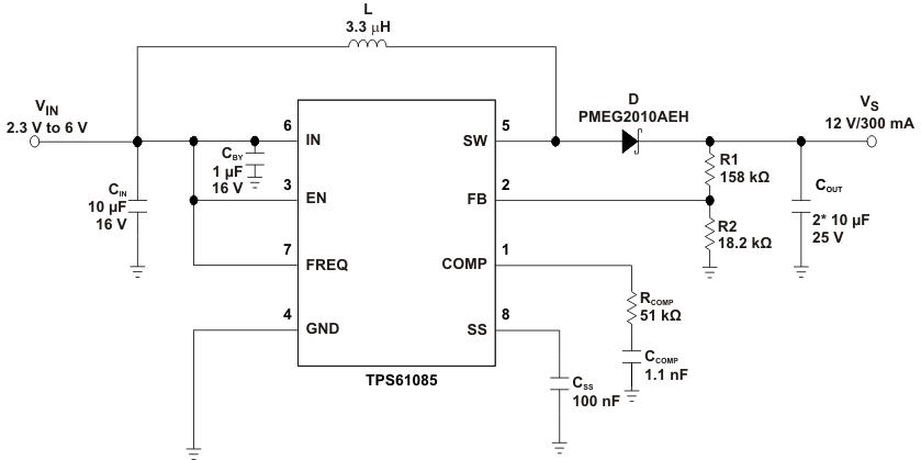
4 Simplified Schematic

typ_app_cir_lvs859.gif