SLVS302B December 2000 – October 2015 TPS60300 , TPS60301 , TPS60302 , TPS60303
PRODUCTION DATA.
- 1 Features
- 2 Applications
- 3 Description
- 4 Revision History
- 5 Description (continued)
- 6 Device Comparison Table
- 7 Pin Configuration and Functions
- 8 Specifications
- 9 Detailed Description
- 10Application and Implementation
- 11Power Supply Recommendations
- 12Layout
- 13Device and Documentation Support
- 14Mechanical, Packaging, and Orderable Information
Package Options
Mechanical Data (Package|Pins)
- DGS|10
Thermal pad, mechanical data (Package|Pins)
Orderable Information
1 Features
- Input Voltage Range From 0.9 V to 1.8 V
- Regulated 3-V or 3.3-V Output Voltage
- Up to 20-mA Output Current
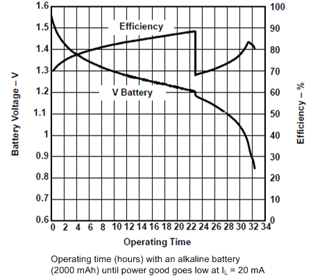
- High Power Conversion Efficiency (up to 90%) Over a Wide Output Current Range, Optimized for 1.2-V Battery Voltage
- Additional Output With 2 Times VIN (OUT1)
- Device Quiescent Current Less Than 35 µA
- Supervisor Included; Open Drain or Push-Pull Power Good Output
- Minimum Number of External Components
- No Inductors Required
- Only Five Small, 1-µF Ceramic Capacitors Required
- Load Isolated From Battery During Shutdown
- Micro-Small 10-Pin MSOP (VSSOP) Package
2 Applications
- Pagers
- Battery-Powered Toys
- Portable Measurement Instruments
- Home-Automation Products
- Medical Instruments (Like Hearing Instruments)
- Metering Applications Using MSP430 Micro-Controller
- Portable Smart Card Readers
3 Description
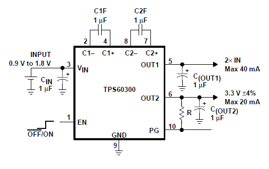
The TPS6030x devices are a family of switched-voltage converters designed specifically for space-critical battery powered applications.
The TPS6030x step-up, regulated charge pumps generate a 3-V (±4%) or 3.3-V (±4%) output voltage from a 0.9-V to 1.8-V input voltage (one alkaline, NiCd, or NiMH battery).
Only five small 1-µF ceramic capacitors are required to build a complete high efficiency DC-DC charge pump converter. To achieve the high efficiency over a wide input voltage range, the charge pump automatically selects between a 3× or 4× conversion mode.
Output 1 (OUT1) can deliver a maximum of 40 mA from a 1-V input, with output 2 (OUT2) not loaded. OUT2 can deliver a maximum of 20 mA from a 1-V input, with OUT1 not loaded. Both outputs can be loaded at the same time, but the total output current of the first voltage doubler must not exceed 40 mA. For example, the load at output 1 is 20 mA and the load at output 2 is 10 mA.
Device Information(1)
| PART NUMBER | PACKAGE | BODY SIZE (MAX) |
|---|---|---|
| TPS60300, TPS60301, TPS60302, TPS60303 |
VSSOP (10) | 3.05 mm × 4.98 mm |
- For all available packages, see the orderable addendum at the end of the data sheet.
Typical Application Schematic

Alkaline Battery Operating Time
