SLVSDT2 November 2016 TPS562219A , TPS563219A
PRODUCTION DATA.
- 1 Features
- 2 Applications
- 3 Description
- 4 Revision History
- 5 Pin Configuration and Functions
- 6 Specifications
- 7 Detailed Description
- 8 Application and Implementation
- 9 Power Supply Recommendations
- 10Layout
- 11Device and Documentation Support
- 12Mechanical, Packaging, and Orderable Information
Package Options
Mechanical Data (Package|Pins)
- DDF|8
Thermal pad, mechanical data (Package|Pins)
Orderable Information
1 Features
- TPS562219A: 2-A Converter With Integrated
133-mΩ and 80-mΩ FETs - TPS563219A: 3-A Converter With Integrated
68-mΩ and 39-mΩ FETs - D-CAP2™ Mode Control with 650-kHz Switching Frequency
- Input Voltage Range: 4.5 V to 17 V
- Output Voltage Range: 0.76 V to 7 V
- 650-kHz Switching Frequency
- Low Shutdown Current Less than 10 µA
- 1% Feedback Voltage Accuracy (25°C)
- Startup from Pre-Biased Output Voltage
- Cycle By Cycle Overcurrent Limit
- Hiccup-mode Under Voltage Protection
- Non-latch OVP, UVLO and TSD Protections
- Adjustable Soft Start
- Power Good Output
2 Applications
- Digital TV Power Supply
- High Definition Blu-ray Disc™ Players
- Networking Home Terminal
- Digital Set Top Box (STB)
3 Description
The TPS562219A and TPS563219A are simple, easy-to-use, 2-A, 3-A synchronous step-down converters in 8 pin SOT-23 package.
The devices are optimized to operate with minimum external component counts and optimized to achieve low standby current.
These switch mode power supply (SMPS) devices employ D-CAP2™ mode control providing a fast transient response and supporting both low equivalent series resistance (ESR) output capacitors such as specialty polymer and ultra-low ESR ceramic capacitors with no external compensation components.
The devices always operate in continuous conduction mode, which reduces the output ripple voltage in light load compared to discontinuous conduction mode . The TPS562219A and TPS563219A are available in a 8-pin 1.6 × 2.9 (mm) SOT (DDF) package, and specified from –40°C to 85°C of ambient temperature.
Device Information(1)
| PART NUMBER | PACKAGE | BODY SIZE (NOM) |
|---|---|---|
| TPS562219A | SOT (8) | 1.60 mm × 2.90 mm |
| TPS563219A |
- For all available packages, see the orderable addendum at the end of the datasheet.
SPACER
SPACER
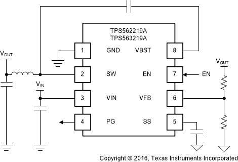
Simplified Schematic

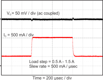
TPS562219A Transient Response
