SLUSCI9A August 2016 – September 2017 TPS549D22
PRODUCTION DATA.
- 1 Features
- 2 Applications
- 3 Description
- 4 Revision History
- 5 Pin Configuration and Functions
- 6 Specifications
-
7 Detailed Description
- 7.1 Overview
- 7.2 Functional Block Diagram
- 7.3 Feature Description
- 7.4 Device Functional Modes
- 7.5
Programming
- 7.5.1 Programmable Pin-Strap Settings
- 7.5.2 Programmable Analog Configurations
- 7.5.3 PMBus Programming
- 7.5.4
Register Maps
- 7.5.4.1 OPERATION Register (address = 1h)
- 7.5.4.2 ON_OFF_CONFIG Register (address = 2h)
- 7.5.4.3 CLEAR FAULTS (address = 3h)
- 7.5.4.4 WRITE PROTECT (address = 10h)
- 7.5.4.5 STORE_DEFAULT_ALL (address = 11h)
- 7.5.4.6 RESTORE_DEFAULT_ALL (address = 12h)
- 7.5.4.7 CAPABILITY (address = 19h)
- 7.5.4.8 VOUT_MODE (address = 20h)
- 7.5.4.9 VOUT_COMMAND (address = 21h)
- 7.5.4.10 VOUT_MARGIN_HIGH (address = 25h)
- 7.5.4.11 VOUT_MARGIN_LOW (address = 26h)
- 7.5.4.12 STATUS_BYTE (address = 78h)
- 7.5.4.13 STATUS_WORD (High Byte) (address = 79h)
- 7.5.4.14 STATUS_VOUT (address = 7Ah)
- 7.5.4.15 STATUS_IOUT (address = 7Bh)
- 7.5.4.16 STATUS_CML (address = 7Eh)
- 7.5.4.17 MFR_SPECIFIC_00 (address = D0h)
- 7.5.4.18 MFR_SPECIFIC_01 (address = D1h)
- 7.5.4.19 MFR_SPECIFIC_02 (address = D2h)
- 7.5.4.20 MFR_SPECIFIC_03 (address = D3h)
- 7.5.4.21 MFR_SPECIFIC_04 (address = D4h)
- 7.5.4.22 MFR_SPECIFIC_06 (address = D6h)
- 7.5.4.23 MFR_SPECIFIC_07 (address = D7h)
- 7.5.4.24 MFR_SPECIFIC_44 (address = FCh)
-
8 Application and Implementation
- 8.1 Application Information
- 8.2
Typical Application: TPS549D22 1.5-V to 16-V Input, 1-V Output, 40-A Converter
- 8.2.1 Design Requirements
- 8.2.2
Detailed Design Procedure
- 8.2.2.1 Custom Design With WEBENCH® Tools
- 8.2.2.2 Switching Frequency Selection
- 8.2.2.3 Inductor Selection
- 8.2.2.4 Output Capacitor Selection
- 8.2.2.5 Input Capacitor Selection
- 8.2.2.6 Bootstrap Capacitor Selection
- 8.2.2.7 BP Pin
- 8.2.2.8 R-C Snubber and VIN Pin High-Frequency Bypass
- 8.2.2.9 Optimize Reference Voltage (VSEL)
- 8.2.2.10 MODE Pin Selection
- 8.2.2.11 ADDR Pin Selection
- 8.2.2.12 Overcurrent Limit Design
- 8.2.3 Application Curves
- 9 Power Supply Recommendations
- 10Layout
- 11Device and Documentation Support
- 12Mechanical, Packaging, and Orderable Information
- 13Package Option Addendum
Package Options
Refer to the PDF data sheet for device specific package drawings
Mechanical Data (Package|Pins)
- RVF|40
Thermal pad, mechanical data (Package|Pins)
- RVF|40
Orderable Information
1 Features
- Input Voltage Range (PVIN): 1.5 V to 16 V
- Input Bias Voltage (VDD) Range: 4.5 V to 22 V
- Output Voltage Range: 0.6 V to 5.5 V
- Integrated, 2.9-mΩ and 1.2-mΩ Power MOSFETs With 40-A Continuous Output Current
- Voltage Reference 0.6 V to 1.2 V in 50-mV Steps Using VSEL Pin
- ±0.5%, 0.9-VREF Tolerance Range: –40°C to +125°C Junction Temperature
- True Differential Remote Sense Amplifier
- D-CAP3™ Control Loop
- Adaptive On-Time Control with 8 PMBusTM Frequency: 315 kHz, 425 kHz, 550 kHz, 650 kHz, 825 kHz, 900 kHz, 1.025 MHz, 1.125 MHz
- Temperature Compensated and Programmable Current Limit with RILIM and OC Clamp
- Choice of Hiccup or Latch-Off OVP or UVP
- VDD UVLO External Adjustment by Precision EN
- Prebias Start-up Support
- Eco-mode™ and FCCM Selectable
- Full Suite of Fault Protection and PGOOD
- Standard VOUT_COMMAND and VOUT_MARGIN (HIGH and LOW)
- Pin-Strapping and On-the-Fly Programming
- Fault Reporting and Warning
- NVM Backup for Selected Commands
- 1-MHz PMBus with PEC and SMB_ALRT#
- Create a Custom Design Using the TPS549D22 With the WEBENCH® Power Designer
2 Applications
- Enterprise Storage, SSD, NAS
- Wireless and Wired Communication Infrastructure
- Industrial PCs, Automation, ATE, PLC, Video Surveillance
- Enterprise Server, Switches, Routers
- ASIC, SoC, FPGA, DSP Core, and I/O Rails
3 Description
The TPS549D22 device is a compact single buck converter with adaptive on-time, D-CAP3 mode control. It is designed for high accuracy, high efficiency, fast transient response, ease-of-use, low external component count and space-conscious power systems.
This device features full differential sense, TI integrated FETs with a high-side on-resistance of 2.9 mΩ and a low-side on-resistance of 1.2 mΩ. The device also features accurate 0.5%, 0.9-V reference with an ambient temperature range between –40°C and +125°C. Competitive features include: very low external component count, accurate load regulation and line regulation, auto-skip or FCCM mode operation, and internal soft-start control.
The TPS549D22 device is available in 7-mm × 5-mm, 40-pin, LQFN-CLIP (RVF) package (RoHs exempt).
Device Information(1)
| PART NUMBER | PACKAGE | BODY SIZE (NOM) |
|---|---|---|
| TPS549D22 | LQFN-CLIP (40) | 7.00 mm × 5.00 mm |
- For all available packages, see the orderable addendum at the end of the data sheet.
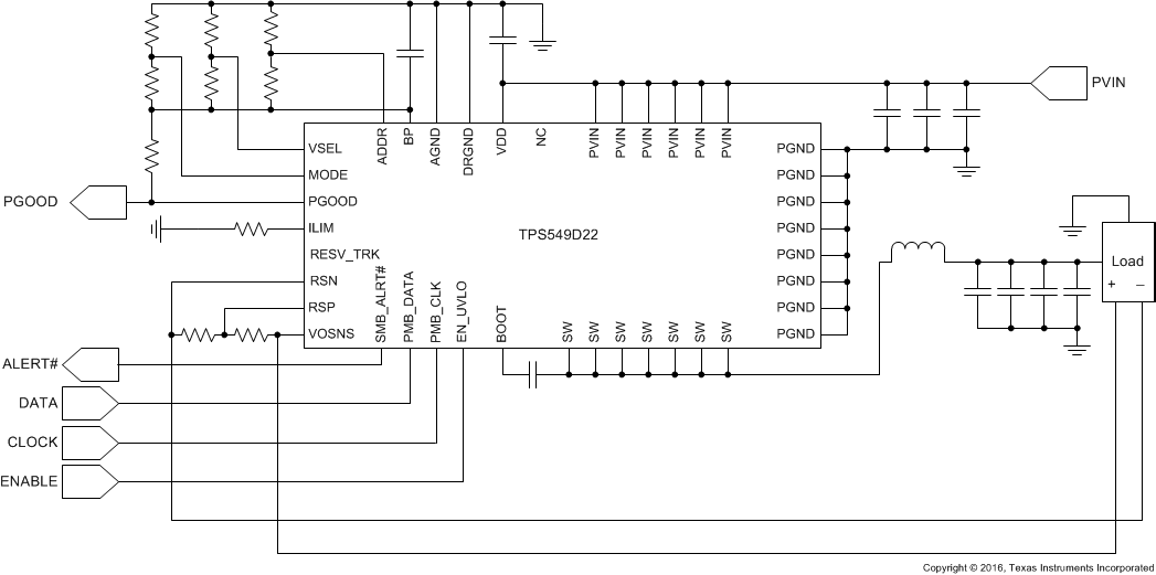
Simplified Application
