SLUSC81 May 2015 TPS544B25 , TPS544C25
PRODUCTION DATA.
- 1 Features
- 2 Applications
- 3 Description
- 4 Revision History
- 5 Device Comparison Table
- 6 Pin Configuration and Functions
- 7 Specifications
-
8 Detailed Description
- 8.1 Overview
- 8.2 Functional Block Diagram
- 8.3
Feature Description
- 8.3.1 Linear Regulators BP3 and BP6
- 8.3.2 Input Undervoltage Lockout (UVLO)
- 8.3.3 Turn-On and Turn-Off Delay and Sequencing
- 8.3.4 Voltage Reference
- 8.3.5 Differential Remote Sense
- 8.3.6 Set Output Voltage and Adapative Voltage Scaling (AVS)
- 8.3.7 Reset VOUT
- 8.3.8 Switching Frequency and Synchronization
- 8.3.9 Soft-Start and TON_RISE Command
- 8.3.10 Pre-Biased Output Start-Up
- 8.3.11 Soft-Stop and TOFF_FALL Command
- 8.3.12 Current Monitoring and Low-Side MOSFET Overcurrent Protection
- 8.3.13 High-Side MOSFET Short-Circuit Protection
- 8.3.14 Over-Temperature Protection
- 8.3.15 Output Overvoltage and Undervoltage Protection
- 8.3.16 TON_MAX Fault
- 8.3.17 Power Good (PGOOD) Indicator
- 8.3.18 Fault Protection Responses
- 8.3.19 Switching Node
- 8.3.20 PMBus General Description
- 8.3.21 PMBus Address
- 8.3.22 PMBus Connections
- 8.3.23 Auto ARA (Alert Response Address) Response
- 8.4 Device Functional Modes
- 8.5 Supported PMBus Commands
- 8.6
Register Maps
- 8.6.1 OPERATION (01h)
- 8.6.2 ON_OFF_CONFIG (02h)
- 8.6.3 CLEAR_FAULTS (03h)
- 8.6.4 WRITE_PROTECT (10h)
- 8.6.5 STORE_DEFAULT_ALL (11h)
- 8.6.6 RESTORE_DEFAULT_ALL (12h)
- 8.6.7 CAPABILITY (19h)
- 8.6.8 SMBALERT_MASK (1Bh)
- 8.6.9 VOUT_MODE (20h)
- 8.6.10 VOUT_COMMAND (21h)
- 8.6.11 VOUT_MAX (24h)
- 8.6.12 VOUT_TRANSITION_RATE (27h)
- 8.6.13 VOUT_SCALE_LOOP (29h)
- 8.6.14 VIN_ON (35h)
- 8.6.15 VIN_OFF (36h)
- 8.6.16 IOUT_CAL_OFFSET (39h)
- 8.6.17 VOUT_OV_FAULT_LIMIT (40h)
- 8.6.18 VOUT_OV_FAULT_RESPONSE (41h)
- 8.6.19 VOUT_OV_WARN_LIMIT (42h)
- 8.6.20 VOUT_UV_WARN_LIMIT (43h)
- 8.6.21 VOUT_UV_FAULT_LIMIT (44h)
- 8.6.22 VOUT_UV_FAULT_RESPONSE (45h)
- 8.6.23 IOUT_OC_FAULT_LIMIT (46h)
- 8.6.24 IOUT_OC_FAULT_RESPONSE (47h)
- 8.6.25 IOUT_OC_WARN_LIMIT (4Ah)
- 8.6.26 OT_FAULT_LIMIT (4Fh)
- 8.6.27 OT_FAULT_RESPONSE (50h)
- 8.6.28 OT_WARN_LIMIT (51h)
- 8.6.29 TON_DELAY (60h)
- 8.6.30 TON_RISE (61h)
- 8.6.31 TON_MAX_FAULT_LIMIT (62h)
- 8.6.32 TON_MAX_FAULT_RESPONSE (63h)
- 8.6.33 TOFF_DELAY (64h)
- 8.6.34 TOFF_FALL (65h)
- 8.6.35 STATUS_BYTE (78h)
- 8.6.36 STATUS_WORD (79h)
- 8.6.37 STATUS_VOUT (7Ah)
- 8.6.38 STATUS_IOUT (7Bh)
- 8.6.39 STATUS_INPUT (7Ch)
- 8.6.40 STATUS_TEMPERATURE (7Dh)
- 8.6.41 STATUS_CML (7Eh)
- 8.6.42 STATUS_MFR_SPECIFIC (80h)
- 8.6.43 READ_VOUT (8Bh)
- 8.6.44 READ_IOUT (8Ch)
- 8.6.45 READ_TEMPERATURE_2 (8Eh)
- 8.6.46 PMBUS_REVISION (98h)
- 8.6.47 MFR_VOUT_MIN (A4h)
- 8.6.48 IC_DEVICE_ID (ADh)
- 8.6.49 IC_DEVICE_REV (AEh)
- 8.6.50 MFR_SPECIFIC_00 (D0h)
- 8.6.51 OPTIONS (MFR_SPECIFIC_21) (E5h)
- 8.6.52 MISC_CONFIG_OPTIONS (MFR_SPECIFIC_32) (F0h)
-
9 Applications and Implementation
- 9.1 Application Information
- 9.2
Typical Applications
- 9.2.1 TPS544C25 4.5-V to 18-V Input, 0.95-V Output, 30-A Converter
- 9.2.2 Design Requirements
- 9.2.3
Design Procedure
- 9.2.3.1 Switching Frequency Selection
- 9.2.3.2 Inductor Selection
- 9.2.3.3 Output Capacitor Selection
- 9.2.3.4 Input Capacitor Selection
- 9.2.3.5 Bootstrap Capacitor Selection
- 9.2.3.6 BP6 and BP3
- 9.2.3.7 R-C Snubber and VIN Pin High-Frequency Bypass
- 9.2.3.8 Temperature Sensor
- 9.2.3.9 Key PMBus Parameter Selection
- 9.2.3.10 Output Voltage Setting and Frequency Compensation Selection
- 9.2.4 Application Curves
- 10Power Supply Recommendations
- 11Layout
- 12Device and Documentation Support
- 13Mechanical, Packaging, and Orderable Information
Package Options
Mechanical Data (Package|Pins)
- RVF|40
Thermal pad, mechanical data (Package|Pins)
- RVF|40
Orderable Information
1 Features
- PMBus 1.2 Compliant Converters: 20 A and 30 A
- Input Voltage Range: 4.5 V to 18 V
- Output Voltage Range: 0.5 V to 5.5 V
- 5 mm × 7 mm LQFN Package
- Single Thermal Pad
- Integrated 5.5-mΩ and 2.0-mΩ Stacked NexFET™ Power Stage
- 500-mV to 1500-mV Reference for Adapative Voltage Scaling (AVS) and Margining through PMBus
- 0.5% Reference Accuracy at 600 mV and Above
- Lossless Low-Side MOSFET Current Sensing
- Voltage Mode Control with Input Feed-Forward
- Differential Remote Sensing
- Monotonic Start-Up into Pre-Biased Output
- Output Voltage and Output Current Reporting
- External Temperature Monitoring with 2N3904 Transistor
- Programmable via the PMBus interface
- VOUT_COMMAND and AVS VOUT Transition Rate
- Overcurrent Protection with Thermal Compensation
- UVLO, Soft-Start and Soft-Stop
- PGOOD, OV, UV, OT Levels
- Fault Responses
- Turn-On and Turn-Off Delays
- Thermal Shutdown
- Pin Strapping for Switching Frequency: 200 kHz to 1 MHz
- Frequency Synchronization to an External Clock
- Footprint Compatible 20-A, 30-A Converters
2 Applications
- Test and Instrumentation
- Ethernet Switches, Optical Switches, Routers, Base Stations
- Servers
- Enterprise Storage SSD
- High-Density Power Solutions
3 Description
The TPS544x25 devices are PMBus 1.2 Compliant, non-isolated DC-DC converters with integrated FETs, capable of high-frequency operation and 20-A or 30-A current output from a 5 mm × 7 mm package. High-frequency, low-loss switching, provided by an integrated NexFET™ power stage and optimized drivers, allows for very high-density power solutions. The PMBus interface enables the AVS through VOUT_COMMAND, flexible converter configuration, as well as key parameters monitoring including output voltage, current and an optional external temperature. Response to fault conditions can be set to either restart, latch-off or ignore depending on system requirements.
Device Information
| DEVICE NAME | PACKAGE | BODY SIZE |
|---|---|---|
| TPS544B25RVFT | LQFN (40) | 5.00 mm × 7.00 mm |
| TPS544C25RVFT | LQFN (40) | 5.00 mm × 7.00 mm |
.
.
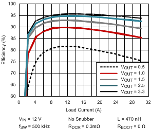
Efficiency

4 Revision History
| DATE | REVISION | NOTES |
|---|---|---|
| May 2015 | * | Initial release. |