SLUSBN5B August 2013 – July 2015 TPS53515
PRODUCTION DATA.
- 1 Features
- 2 Applications
- 3 Description
- 4 Revision History
- 5 Pin Configuration and Functions
- 6 Specifications
-
7 Detailed Description
- 7.1 Overview
- 7.2 Functional Block Diagram
- 7.3
Feature Description
- 7.3.1 5-V LDO and VREG Start-Up
- 7.3.2 Enable, Soft Start, and Mode Selection
- 7.3.3 Frequency Selection
- 7.3.4 D-CAP3 Control and Mode Selection
- 7.3.5 Power-Good
- 7.3.6 Current Sense and Overcurrent Protection
- 7.3.7 Overvoltage and Undervoltage Protection
- 7.3.8 Out-of-Bounds Operation
- 7.3.9 UVLO Protection
- 7.3.10 Thermal Shutdown
- 7.4 Device Functional Modes
- 8 Application and Implementation
- 9 Power Supply Recommendations
- 10Layout
- 11Device and Documentation Support
- 12Mechanical, Packaging, and Orderable Information
Package Options
Mechanical Data (Package|Pins)
- RVE|28
Thermal pad, mechanical data (Package|Pins)
- RVE|28
Orderable Information
1 Features
- Integrated 13.8-mΩ and 5.9-mΩ MOSFETs With
12-A Continuous Output Current - Supports All Ceramic Output Capacitors
- Reference Voltage 600 mV ±0.5% Tolerance
- Output Voltage Range: 0.6 V to 5.5 V
- D-CAP3™ Control Mode With Fast Load-Step ResponseSWIFT™
- Auto-Skipping Eco-mode™ for High Light-Load Efficiency
- FCCM for Tight Output Ripple and Voltage Requirements
- Eight Selectable Frequency Settings from
250 kHz to 1 MHz - Precharged Startup Capability
- Built-in Output Discharge Circuit
- Open-Drain Power-Good Output
- 3.5 mm × 4.5 mm, 28-Pin, VQFN-CLIP Package
2 Applications
- Server and Cloud-Computing POLs
- Broadband, Networking, and Optical Communications Infrastructure
- I/O Supplies
- Supported at the WEBENCH® Design Center
3 Description
The TPS53515 device is a small-sized, synchronous buck converter with an adaptive on-time D-CAP3 control mode. The device offers ease-of-use and low external-component count for space-conscious power systems.
This device features high-performance integrated MOSFETs, accurate 0.5% 0.6-V reference, and an integrated boost switch. Competitive features include very low external-component count, fast load-transient response, auto-skip mode operation, internal soft-start control, and no requirement for compensation.
A forced continuous conduction mode helps meet tight voltage regulation accuracy requirements for performance DSPs and FPGAs. The TPS53515 device is available in a 28-pin VQFN-CLIP package and is specified from –40°C to 85°C ambient temperature.
Device Information (1)
| PART NUMBER | PACKAGE | BODY SIZE (NOM) |
|---|---|---|
| TPS53515 | VQFN-CLIP (28) | 4.50 mm × 3.50 mm |
- For all available packages, see the orderable addendum at the end of the datasheet.
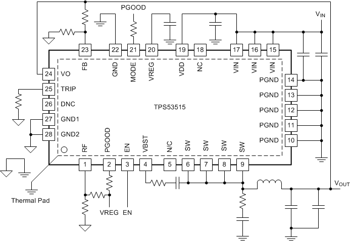
Simplified Schematic

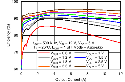
Efficiency
