SLUSAS8A December 2011 – October 2016 TPS53313
PRODUCTION DATA.
- 1 Features
- 2 Applications
- 3 Description
- 4 Revision History
- 5 Pin Configuration and Functions
- 6 Specifications
- 7 Detailed Description
- 8 Application and Implementation
- 9 Power Supply Recommendations
- 10Layout
- 11Device and Documentation Support
- 12Mechanical, Packaging, and Orderable Information
Package Options
Mechanical Data (Package|Pins)
- RGE|24
Thermal pad, mechanical data (Package|Pins)
- RGE|24
Orderable Information
1 Features
- 4.5-V to 16-V Conversion Voltage Range
- Adjustable Output Voltage Ranging from 0.6 V to 0.7 × VIN
- Continuous 6-A Output Current
- Supports All MLCC Output Capacitors
- Selectable SKIP Mode or Forced CCM
- Selectable Soft-Start Time (1 ms, 3 ms, or 6 ms)
- Selectable 4-5 A, 6-A or 9-A Peak Current Limit
- Optimized Efficiency at Light and Heavy Loads
- Voltage Mode Control
- Programmable Switching Frequency from 250 kHz to 1.5 MHz
- Synchronizes to External Clock
- RDS(on) Sensing for Zero Crossing Detection and Overcurrent Protection
- Soft-Stop Output Discharge During Disable
- Overcurrent, Overvoltage, and Undervoltage Protection With Hiccup
- Overtemperature Protection
- Open-Drain, Power Good Indication
- Internal Bootstrap Switch
- 4 mm × 4 mm, 24-Pin VQFN Package
2 Applications
- POL Applications for 5-V
- 12-V Step-Down Rails
3 Description
TPS53313 provides a 5-V or 12-V synchronous buck converter that integrates two N-Channel MOSFETs. Due to low RDS(on) and TI proprietary SmoothPWM™ skip mode of operation, it optimizes the efficiency at light-load condition without compromising the output voltage ripple.
The TPS53313 features programmable (from 250 kHz to 1.5 MHz) switching frequency with selectable skip mode or forced CCM mode operation. The device provides prebiased startup, soft-stop, integrated bootstrap switch, power good function, and EN/input UVLO protection. It supports input voltages from 4.5 V to 16 V and no extra bias voltage is needed. The output voltage is adjustable from 0.6 V up to 0.7 × VIN.
The TPS53313 is available in a 4 mm × 4 mm, 24-pin VQFN package (Green RoHs compliant and Pb free) and operates from –40°C to 85°C.
Device Information(1)
| PART NUMBER | PACKAGE | BODY SIZE (NOM) |
|---|---|---|
| TPS53313 | VQFN (24) | 4.00 mm × 4.00 mm |
- For all available packages, see the orderable addendum at the end of the data sheet.
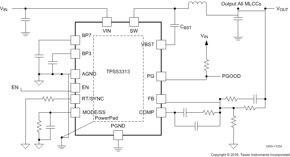
Typical Application Circuit
