SLVSAU0G May 2011 – December 2015 TPD4S014
PRODUCTION DATA.
- 1 Features
- 2 Applications
- 3 Description
- 4 Revision History
- 5 Pin Configuration and Functions
- 6 Specifications
-
7 Detailed Description
- 7.1 Overview
- 7.2 Functional Block Diagram
- 7.3
Feature Description
- 7.3.1 Input Voltage Protection at VBUS up to 28 V DC
- 7.3.2 Low RON nFET Switch
- 7.3.3 ESD Performance D+/D-/ID/VBUS Pins
- 7.3.4 Overvoltage and Undervoltage Lockout Features
- 7.3.5 Capacitance TVS ESD Clamp for USB2.0 Hi-Speed Data Rate
- 7.3.6 Start-up Delay
- 7.3.7 OVP Glitch Immunity
- 7.3.8 Integrated Input Enable and Status Output Signal
- 7.3.9 Thermal Shutdown
- 7.4 Device Functional Modes
- 8 Application and Implementation
- 9 Power Supply Recommendations
- 10Layout
- 11Device and Documentation Support
- 12Mechanical, Packaging, and Orderable Information
Package Options
Mechanical Data (Package|Pins)
- DSQ|10
Thermal pad, mechanical data (Package|Pins)
Orderable Information
1 Features
- Input Voltage Protection at VBUS up to 28 V
- Low Ron nFET Switch
- Supports > 2 A Charging Current
- ESD Performance D+/D–/ID/VBUS Pins:
- ±15-kV Contact Discharge (IEC 61000-4-2)
- ±15-kV Air Gap Discharge (IEC 61000-4-2)
- Overvoltage and Undervoltage Lockout Features
- Low Capacitance TVS ESD Clamp for USB2.0 High Speed Data Rate
- Internal 17 ms Startup Delay
- Integrated Input Enable and Status Output Signal
- Thermal Shutdown Feature
- Space Saving SON Package (2 mm × 2 mm)
2 Applications
- Cell Phones
- eBook
- Portable Media Players
- Digital Camera
3 Description
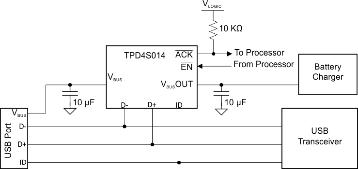
The TPD4S014 is a single-chip solution for USB charger port protection. This device offers low capacitance transient voltage suppressor (TVS) electrostatic discharge (ESD) clamps for the D+, D–, and standard capacitance for the ID pin. On the VBUS pin, this device provides overvoltage protection (OVP) up to 28 V DC. The overvoltage lockout feature ensures that if there is a fault condition at the VBUS line, the TPD4S014 is able to isolate the VBUS line to protect the internal circuitry from damage. There is a 17-ms turn-on delay after VBUS rises above the undervoltage lockout (UVLO) threshold in order to let the voltage stabilize before turning the nFET on. This function acts as a de-glitch and prevents unnecessary switching if there is any ringing on the line during connection.
Device Information(1)
| PART NUMBER | PACKAGE | BODY SIZE (NOM) |
|---|---|---|
| TPD4S014 | WSON (10) | 2.00 mm x 2.00 mm |
- For all available packages, see the orderable addendum at the end of the data sheet.
Simplified Block Diagram
