SBOS321E March 2005 – April 2016 TLV3501 , TLV3502
PRODUCTION DATA.
- 1 Features
- 2 Applications
- 3 Description
- 4 Revision History
- 5 Pin Configuration and Functions
- 6 Specifications
- 7 Detailed Description
- 8 Application and Implementation
- 9 Power Supply Recommendations
- 10Layout
- 11Device and Documentation Support
- 12Mechanical, Packaging, and Orderable Information
Package Options
Mechanical Data (Package|Pins)
Thermal pad, mechanical data (Package|Pins)
- DCN|8
Orderable Information
1 Features
2 Applications
- Automatic Test Equipment
- Wireless Base Stations
- Threshold Detectors
- Zero-Crossing Detectors
- Window Comparators
3 Description
The TLV350x family of push-pull output comparators feature a fast 4.5-ns propagation delay and operation from 2.7 V to 5.5 V. Beyond-the-rails input common-mode range makes it an ideal choice for low-voltage applications. The rail-to-rail output directly drives either CMOS or TTL logic.
Microsize packages provide options for portable and space-restricted applications. The single (TLV3501) is available in 6-pin SOT-23 and 8-pin SO packages. The dual (TLV3502) comes in the 8-pin SOT-23 and 8-pin SO packages.
Device Information(1)
| PART NUMBER | PACKAGE | BODY SIZE (NOM) |
|---|---|---|
| TLV3501 | SOT-23 (6) | 1.60 mm × 2.90 mm |
| SOIC (8) | 3.91 mm × 4.90 mm | |
| TLV3502 | SOT-23 (8) | 1.63 mm × 2.90 mm |
| SOIC (8) | 3.91 mm × 4.90 mm |
- For all available packages, see the orderable addendum at the end of the data sheet.
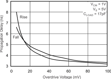
Propagation Delay vs Overdrive Voltage
