SBOS262E December 2002 – December 2016 TLV3491 , TLV3492 , TLV3494
PRODUCTION DATA.
- 1 Features
- 2 Applications
- 3 Description
- 4 Revision History
- 5 Device Comparison Table
- 6 Pin Configuration and Functions
- 7 Specifications
- 8 Detailed Description
- 9 Application and Implementation
- 10Power Supply Recommendations
- 11Layout
- 12Device and Documentation Support
- 13Mechanical, Packaging, and Orderable Information
Package Options
Mechanical Data (Package|Pins)
Thermal pad, mechanical data (Package|Pins)
Orderable Information
1 Features
- Very Low Supply Current: 0.8 µA (Typical)
- Input Common-Mode Range: 200-mV Beyond Supply Rails
- Supply Voltage: 1.8 V to 5.5 V
- High Speed: 6 µs
- Push-Pull CMOS Output Stage
- Small Packages:
- 5-Pin SOT-23 (Single)
- 8-Pin SOT-23 (Dual)
2 Applications
- Portable Medical Equipment
- Wireless Security Systems
- Remote Control Systems
- Handheld Instruments
- Ultra-Low Power Systems
3 Description
The TLV349x family of push-pull output comparators features a fast 6-µs response time and < 1.2-µA (maximum) nanopower capability, allowing operation from 1.8 V to 5.5 V. Input common-mode range beyond supply rails make the TLV349x an ideal choice for low-voltage applications.
Micro-sized packages provide options for portable and space-restricted applications. The single (TLV3491) is available in 5-pin SOT-23 and 8-pin SOIC packages. The dual (TLV3492) comes in 8-pin SOT-23 and SOIC packages. The quad (TLV3494) is available in both 14-pin TSSOP and SOIC packages.
The TLV349x is excellent for power-sensitive, low-voltage (two-cell) applications.
Device Information(1)
| PART NUMBER | PACKAGE | BODY SIZE (NOM) |
|---|---|---|
| TLV3491 | SOT-23 (5) | 2.90 mm × 1.60 mm |
| SOIC (8) | 4.90 mm × 3.91 mm | |
| TLV3492 | SOT-23 (8) | 2.90 mm × 1.63 mm |
| SOIC (8) | 4.90 mm × 3.91 mm | |
| TLV3494 | SOIC (14) | 8.65 mm × 3.91 mm |
| TSSOP (14) | 5.00 mm × 4.40 mm |
- For all available packages, see the orderable addendum at the end of the data sheet.
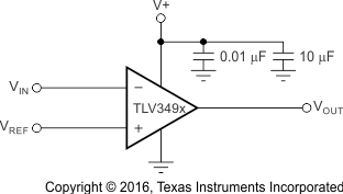
TLV349x Basic Connections
