SLOS351E February 2004 – November 2016 TLV271 , TLV272 , TLV274
PRODUCTION DATA.
- 1 Features
- 2 Applications
- 3 Description
- 4 Revision History
- 5 Device Comparison Table
- 6 Pin Configuration and Functions
-
7 Specifications
- 7.1 Absolute Maximum Ratings
- 7.2 Recommended Operating Conditions
- 7.3 Thermal Information: TLV271
- 7.4 Thermal Information: TLV272
- 7.5 Thermal Information: TLV274
- 7.6 Electrical Characteristics: DC Characteristics
- 7.7 Electrical Characteristics: Input Characteristics
- 7.8 Electrical Characteristics: Output Characteristics
- 7.9 Electrical Characteristics: Power Supply
- 7.10 Electrical Characteristics: Dynamic Performance
- 7.11 Electrical Characteristics: Noise/Distortion Performance
- 7.12 Typical Characteristics
- 8 Detailed Description
- 9 Application and Implementation
- 10Power Supply Recommendations
- 11Layout
- 12Device and Documentation Support
- 13Mechanical, Packaging, and Orderable Information
Package Options
Refer to the PDF data sheet for device specific package drawings
Mechanical Data (Package|Pins)
- D|8
- P|8
- DGK|8
Thermal pad, mechanical data (Package|Pins)
Orderable Information
1 Features
- Rail-to-Rail Output
- Wide Bandwidth: 3 MHz
- High Slew Rate: 2.4 V/µs
- Supply Voltage Range: 2.7 V to 16 V
- Supply Current: 550 µA/Channel
- Input Noise Voltage: 39 nV/√Hz
- Input Bias Current: 1 pA
- Specified Temperature Range:
- Commercial Grade: 0°C to 70°C
- Industrial Grade: −40°C to 125°C
- Ultrasmall Packaging:
- 5-Pin SOT-23 (TLV271)
- 8-Pin MSOP (TLV272)
- Ideal Upgrade for TLC72x Family
2 Applications
- E-Bike
- Power Banks
- Smoke detectors
- Solar Inverters
- Low-Power Motor Controls
- Battery-Powered Instruments
- Building Automation
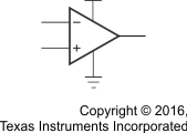
Operational Amplifier

3 Description
Operating from 2.7 V to 16 V over the extended industrial temperature range from -40°C to +125°C, the TLV27x is a low power, wide bandwidth operational amplifier (opamp) with rail to rail output. This makes it an ideal alternative to the TLC27x family for applications where rail-to-rail output swings are essential. The TLV27x provides 3-MHz bandwidth from only 550 µA.
Like the TLC27x, the TLV27x is fully specified for 5-V and ±5-V supplies. The maximum recommended supply voltage is 16 V, which allows the devices to be operated from a variety of rechargeable cells (±8 V supplies down to ±1.35 V).
The CMOS inputs enable use in high-impedance sensor interfaces, with the lower voltage operation making an attractive alternative for the TLC27x in battery-powered applications.
All members are available in PDIP and SOIC with the singles in the small SOT-23 package, duals in the MSOP, and quads in the TSSOP package.
The 2.7-V operation makes it compatible with Li-Ion powered systems and the operating supply voltage range of many micropower microcontrollers available today including TI’s MSP430.
Device Information(1)
| PART NUMBER | PACKAGE | BODY SIZE (NOM) |
|---|---|---|
| TLV271 | SOIC (8) | 4.98 mm × 3.91 mm |
| SOT-23 (5) | 2.90 mm × 1.60 mm | |
| PDIP (8) | 9.81 mm × 6.35 mm | |
| TLV272 | SOIC (8) | 4.98 mm × 3.91 mm |
| PDIP (8) | 9.81 mm × 6.35 mm | |
| VSSOP (8) | 3.00 mm × 3.00 mm | |
| TLV274 | SOIC (14) | 8.65 mm × 3.91 mm |
| PDIP (14) | 3.90 mm × 6.35 mm | |
| TSSOP (14) | 5.00 mm × 4.40 mm |
- For all available packages, see the orderable addendum at the end of the data sheet.