SLVS067M March 1992 – November 2016 TLV2217
PRODUCTION DATA.
- 1 Features
- 2 Applications
- 3 Description
- 4 Revision History
- 5 Pin Configuration and Functions
- 6 Specifications
- 7 Detailed Description
- 8 Application and Implementation
- 9 Power Supply Recommendations
- 10Layout
- 11Device and Documentation Support
- 12Mechanical, Packaging, and Orderable Information
Package Options
Refer to the PDF data sheet for device specific package drawings
Mechanical Data (Package|Pins)
- KVU|3
- KCS|3
- PW|20
Thermal pad, mechanical data (Package|Pins)
- KVU|3
Orderable Information
1 Features
- Fixed 1.8-V, 2.5-V, and 3.3-V Outputs
- ±1% Maximum Output Voltage Tolerance at
TJ = 25°C - 500-mV Maximum Dropout Voltage at 500 mA (3.3-V Option)
- ±2% Output Voltage Variation Across Load and Temperature
- Internal Overcurrent Limiting
- Internal Thermal-Overload Protection
- Internal Overvoltage Protection
2 Applications
- Electronic Points of Sale
- Medical, Health, and Fitness Applications
- Printers
- Appliances and White Goods
- TV Set-Top Boxes
3 Description
The TLV2217 family of low-dropout regulators offers a variety of fixed-voltage options that offer a maximum continuous input voltage of 16 V, making them more versatile than CMOS regulators. Utilizing a PNP pass element, these regulators are capable of sourcing 500 mA of current, with a specified maximum dropout of 500 mV (3.3-V and 2.5-V options), making these regulators ideal for low-voltage applications. Additionally, the TLV2217 regulators offer very tight output accuracy of ±2% across operating load and temperature ranges. Other convenient features the regulators provide are internal overcurrent limiting, thermal-overload protection, and overvoltage protection. The TLV2217 family of regulators is available in fixed voltages of 1.8 V, 2.5 V, and 3.3 V.
Device Information(1)
| PART NUMBER | PACKAGE | BODY SIZE (NOM) |
|---|---|---|
| TLV2217-xxPW | TSSOP (20) | 6.50 mm × 4.40 mm |
| TLV2217-xxKVU | TO-252 (2) | 6.04 mm × 6.15 mm |
| TLV2217-xxKCS | TO-220 (3) | 10.16 mm × 9.15 mm |
- For all available packages, see the orderable addendum at the end of the data sheet.
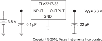
Typical Application
