SBOS589D December 2013 – June 2015 TLV1701 , TLV1702 , TLV1704
PRODUCTION DATA.
- 1 Features
- 2 Applications
- 3 Description
- 4 Revision History
- 5 Device Comparison
- 6 Pin Configuration and Functions
- 7 Specifications
- 8 Detailed Description
- 9 Applications and Implementation
- 10Power Supply Recommendations
- 11Layout
- 12Device and Documentation Support
- 13Mechanical, Packaging, and Orderable Information
Package Options
Mechanical Data (Package|Pins)
- PW|14
Thermal pad, mechanical data (Package|Pins)
Orderable Information
1 Features
-
Supply Range:
+2.2 V to +36 V or ±1.1 V to ±18 V - Low Quiescent Current:
55 µA per Comparator - Input Common-Mode Range Includes Both Rails
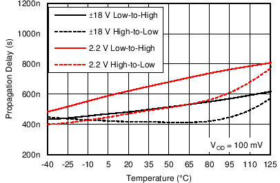
- Low Propagation Delay: 560 ns
- Low Input Offset Voltage: 300 µV
- Open Collector Outputs:
- Industrial Temperature Range:
–40°C to +125°C - Small Packages:
- Single: SC70-5, SOT-23-5, SOT553-5
- Dual: VSSOP-8, X2QFN-8
- Quad: TSSOP-14
2 Applications
- Overvoltage and Undervoltage Detectors
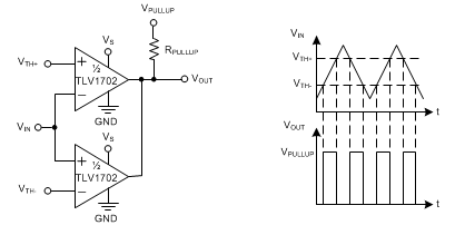
- Window Comparators
- Overcurrent Detectors
- Zero-Crossing Detectors
- System Monitoring for:
- Power Supplies
- White Goods
- Industrial Sensors
- Automotive
- Medical
3 Description
The TLV170x family of devices offers a wide supply range, rail-to-rail inputs, low quiescent current, and low propagation delay. All these features come in industry-standard, extremely-small packages, making these devices the best general-purpose comparators available.
The open collector output offers the advantage of allowing the output to be pulled to any voltage rail up to +36 V above the negative power supply, regardless of the TLV170x supply voltage.
These devices are available in single (TLV1701), dual (TLV1702), and quad (TLV1704) channel versions. Low input offset voltage, low input bias currents, low supply current, and open-collector configuration make the TLV170x family flexible enough to handle almost any application, from simple voltage detection to driving a single relay.
All devices are specified for operation across the expanded industrial temperature range of –40°C to +125°C.
Device Information(1)
| PART NUMBER | PACKAGE | BODY SIZE (NOM) |
|---|---|---|
| TLV1701 | SOT553 (5) | 1.20 mm × 1.60 mm |
| SC-70 (5) | 1.25 mm × 2.00 mm | |
| SOT-23 (5) | 1.60 mm × 2.90 mm | |
| TLV1702 | X2QFN (8) | 1.50 mm × 1.50 mm |
| VSSOP (8)(2) | 3.00 mm × 3.00 mm | |
| TLV1704 | TSSOP (14) | 4.40 mm × 5.00 mm |
- For all available packages, see the package option addendum at the end of the datasheet.
- The VSSOP package is the same as the MSOP package.

