SBOS832A July 2017 – August 2017 TLV07
PRODUCTION DATA.
- 1 Features
- 2 Applications
- 3 Description
- 4 Revision History
- 5 Pin Configuration and Functions
- 6 Specifications
- 7 Detailed Description
- 8 Application and Implementation
- 9 Power Supply Recommendations
- 10Layout
- 11Device and Documentation Support
- 12Mechanical, Packaging, and Orderable Information
Package Options
Mechanical Data (Package|Pins)
- D|8
Thermal pad, mechanical data (Package|Pins)
Orderable Information
1 Features
- Low Offset Voltage: 100 µV (Maximum)
- Rail-to-Rail Output
- Low Noise: 19 nV / √Hz
- Unity-Gain Stable
- RFI Filtered Inputs
- Input Range Includes Negative Supply
- Rail-to-Rail Output
- Gain Bandwidth: 1 MHz
- Low Quiescent Current: 930 µA
- Full Industrial Temperature Range:
–40°C to +125°C - Offered in the Industry-Standard 8-Pin SOIC Package
2 Applications
- Battery Testers
- Tracking Amplifier in Power Modules
- Merchant Power Supplies
- Transducer Amplifiers
- Temperature Measurements
- Strain Gauge Amplifiers
3 Description
The TLV07 device is a 36-V, single-supply, low-noise, precision operational amplifier (op amp) manufactured using TI’s laser trim operational amplifier technology. Each amplifiers' input offset voltage is trimmed in production to obtain a low offset voltage of 100 µV (maximum).
The TLV07 offers outstanding dc precision and ac performance, including rail-to-rail output, low offset voltage (±100 µV, maximum) and 1-MHz bandwidth. The TLV07 is stable at G = 1 with capacitive loads up to 200 pF. The input can operate 100 mV below the negative rail and within 2 V of the positive rail. This wide input voltage range, combined with a high CMRR of 120 dB, make the TLV07 well-suited when operated in the non-inverting configuration.
The TLV07 op amp is specified from –40°C to +125°C.
Device Information(1)
| PART NUMBER | PACKAGE | BODY SIZE (NOM) |
|---|---|---|
| TLV07 | SOIC (8) | 4.90 mm × 3.91 mm |
- For all available packages, see the orderable addendum at the end of the data sheet.
space
space
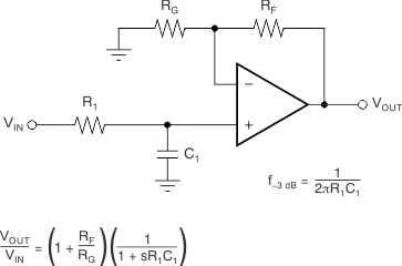
Single Pole Low-Pass Filter With Gain
