SCLS467F FEBRUARY 2003 – June 2016 SN74LV123A-Q1
PRODUCTION DATA.
- 1 Features
- 2 Applications
- 3 Description
- 4 Revision History
- 5 Pin Configuration and Functions
-
6 Specifications
- 6.1 Absolute Maximum Ratings
- 6.2 ESD Ratings
- 6.3 Recommended Operating Conditions
- 6.4 Thermal Information
- 6.5 Electrical Characteristics
- 6.6 Timing Requirements — VCC = 3.3 V ± 0.3 V
- 6.7 Timing Requirements — VCC = 5 V ± 0.5 V
- 6.8 Switching Characteristics — VCC = 3.3 V ± 0.3 V
- 6.9 Switching Characteristics — VCC = 5 V ± 0.5 V
- 6.10 Operating Characteristics
- 6.11 Typical Characteristics
- 7 Parameter Measurement Information
- 8 Detailed Description
- 9 Application and Implementation
- 10Power Supply Recommendations
- 11Layout
- 12Device and Documentation Support
- 13Mechanical, Packaging, and Orderable Information
Package Options
Refer to the PDF data sheet for device specific package drawings
Mechanical Data (Package|Pins)
- PW|16
Thermal pad, mechanical data (Package|Pins)
Orderable Information
1 Features
- Qualified for Automotive Applications
- Typical VOLP (Output Ground Bounce)
<0.8 V at VCC = 3.3 V, TA = 25°C - Typical VOHV (Output VOH Undershoot)
>2.3 V at VCC = 3.3 V, TA = 25°C - Supports Mixed-Mode Voltage Operation on All Ports
- Schmitt-Trigger Circuitry on A, B, and CLR Inputs for Slow Input Transition Rates
- Edge Triggered From Active-High or Active-Low Gated Logic Inputs
- Ioff Supports Partial-Power-Down Mode Operation
- Retriggerable for Very Long Output Pulses, up to 100% Duty Cycle
- Overriding Clear Terminates Output Pulse
- Glitch-Free Power-Up Reset on Outputs
- ESD Protection Exceeds JESD 22
2 Applications
3 Description
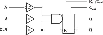
The SN74LV123A-Q1 device is a dual retriggerable monostable multivibrator designed for 2-V to 5.5-V VCC operation.
Device Information(1)
| PART NUMBER | PACKAGE | BODY SIZE (NOM) |
|---|---|---|
| SN74LV123A-Q1 | TSSOP (16) | 5.00 mm × 4.40 mm |
- For all available packages, see the orderable addendum at the end of the datasheet.
