SLLS877H December 2007 – March 2017 SN65HVD1780 , SN65HVD1781 , SN65HVD1782
PRODUCTION DATA.
- 1 Features
- 2 Applications
- 3 Description
- 4 Revision History
- 5 Device Comparison Table
- 6 Pin Configuration and Functions
- 7 Specifications
- 8 Parameter Measurement Information
- 9 Detailed Description
- 10Application and Implementation
- 11Power Supply Recommendations
- 12Layout
- 13Device and Documentation Support
- 14Mechanical, Packaging, and Orderable Information
Package Options
Mechanical Data (Package|Pins)
Thermal pad, mechanical data (Package|Pins)
Orderable Information
1 Features
- Bus-Pin Fault Protection to:
- > ±70 V (SN65HVD1780, SN65HVD1781)
- > ±30 V (SN65HVD1782)
- Operation With 3.3-V to 5-V Supply Range
- ±16-kV HBM Protection on Bus Pins
- Reduced Unit Load for Up to 320 Nodes
- Failsafe Receiver for Open-Circuit, Short-Circuit, and Idle-Bus Conditions
- Low Power Consumption
- Low Standby Supply Current, 1 µA Maximum
- ICC 4-mA Quiescent Current During Operation
- Pin-Compatible With Industry-Standard SN75176
- Signaling Rates of 115 kbps, 1 Mbps, and up to 10 Mbps
- Create a Custom Design using the SN65HVD178x with the WEBENCH® Power Designer
2 Applications
- HVAC Networks
- Security Electronics
- Building Automation
- Telecommunication Equipment
- Motion Control
- Industrial Networks
3 Description
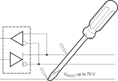
The SN65HVD178x devices are designed to survive overvoltage faults such as direct shorts to power supplies, mis-wiring faults, connector failures, cable crushes, and tool mis-applications. The devices are also robust to ESD events with high levels of protection to the human-body-model specification.
The SN65HVD178x devices combine a differential driver and a differential receiver, which operate from a single power supply. In the SN65HVD1782, the driver differential outputs and the receiver differential inputs are connected internally to form a bus port suitable for half-duplex (two-wire bus) communication. This port features a wide common-mode voltage range, making the devices suitable for multipoint applications over long cable runs. These devices are characterized from –40°C to 125°C. These devices are pin-compatible with the industry-standard SN75176 transceiver, making them drop-in upgrades in most systems.
These devices are fully compliant with ANSI TIA/EIA 485-A with a 5-V supply and can operate with a 3.3-V supply with reduced driver output voltage for low-power applications. For applications where operation is required over an extended common-mode voltage range, see the SN65HVD1785 (SLLS872) data sheet.
Device Information(1)
| PART NUMBER | PACKAGE | BODY SIZE (NOM) |
|---|---|---|
| SN65HVD178x | SOIC (8) | 4.90 mm × 3.91 mm |
| PDIP (8) | 9.81 mm × 6.35 mm |
- For all available packages, see the orderable addendum at the end of the data sheet.
Protection Against Bus Shorts
