SBOS869 July 2017 OPA196 , OPA2196 , OPA4196
PRODUCTION DATA.
- 1 Features
- 2 Applications
- 3 Description
- 4 Revision History
- 5 Pin Configuration and Functions
-
6 Specifications
- 6.1 Absolute Maximum Ratings
- 6.2 ESD Ratings
- 6.3 Recommended Operating Conditions
- 6.4 Thermal Information: OPA196
- 6.5 Thermal Information: OPA2196
- 6.6 Thermal Information: OPA4196
- 6.7 Electrical Characteristics: VS = ±4 V to ±18 V (VS = 8 V to 36 V)
- 6.8 Electrical Characteristics: VS = ±2.25 V to ±4 V (VS = 4.5 V to 8 V)
- 6.9 Typical Characteristics
- 7 Detailed Description
- 8 Application and Implementation
- 9 Power-Supply Recommendations
- 10Layout
- 11Device and Documentation Support
- 12Mechanical, Packaging, and Orderable Information
Package Options
Mechanical Data (Package|Pins)
Thermal pad, mechanical data (Package|Pins)
Orderable Information
1 Features
- Low Offset Voltage: ±100 µV (maximum)
- Low Offset Voltage Drift: ±0.5 µV/°C (typical)
- Low Bias Current: ±5 pA (typical)
- High Common-Mode Rejection: 140 dB
- Low Noise: 15 nV/√Hz at 1 kHz
- Rail-to-Rail Input and Output
- Differential Input Voltage Range to Supply Rail
- Wide Bandwidth: 2.5-MHz GBW
- Low Quiescent Current: 140 µA per Amplifier (typical)
- Wide Supply: ±2.25 V to ±18 V, 4.5 V to 36 V
- EMI/RFI Filtered Inputs
- High Capacitive Load Drive Capability: 1 nF
- Industry Standard Packages:
- Single in SOIC-8, SOT-5, and VSSOP-8
- Dual in SOIC-8 and VSSOP-8
- Quad in SOIC-14, TSSOP-14, and QFN-16
2 Applications
- Multiplexed Data-Acquisition Systems
- Test and Measurement Equipment
- High-Resolution ADC Driver Amplifiers
- SAR ADC Reference Buffers
- Analog Input and Output Modules
- High-Side and Low-Side Current Sensing
- High-Precision Comparator
- Medical Instrumentation
3 Description
The OPAx196 family (OPA196, OPA2196, and OPA4196) is a new generation of 36-V, rail-to-rail e-trim™ operational amplifiers (op amps).
These devices offer very low offset voltage (±25 μV, typical), drift (±0.5 μV/°C, typical), and low bias current (±5 pA, typical) combined with very low quiescent current (140 μA/channel, typical) across the entire output range.
Unique features, such as differential input-voltage range to the supply rail, high output current (±65 mA), and high capacitive load drive of up to 1 nF make the OPAx196 a robust, high-performance operational amplifier for high-voltage industrial applications.
The OPAx196 family of op amps is available in standard packages and is specified from –40°C to +125°C.
Device Information(1)
| PART NUMBER | PACKAGE | BODY SIZE (NOM) |
|---|---|---|
| OPA196 | SOIC (8) | 4.90 mm × 3.90 mm |
| SOT (5) | 2.90 mm × 1.60 mm | |
| VSSOP (8) | 3.00 mm × 3.00 mm | |
| OPA2196 | SOIC (8) | 4.90 mm × 3.90 mm |
| VSSOP (8) | 3.00 mm × 3.00 mm | |
| OPA4196 | SOIC (14) | 8.65 mm x 3.90 mm |
| TSSOP (14) | 5.00 mm x 4.40 mm |
- For all available packages, see the package option addendum at the end of the data sheet.
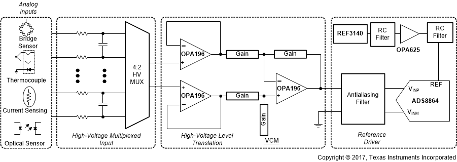
OPA196 in a High-Voltage, Multiplexed, Data-Acquisition System
