SBOS860 April 2017 OPA188-Q1 , OPA2188-Q1
PRODUCTION DATA.
- 1 Features
- 2 Applications
- 3 Description
- 4 Revision History
- 5 Device Comparison Table
- 6 Pin Configuration and Functions
- 7 Specifications
- 8 Detailed Description
- 9 Application and Implementation
- 10Power Supply Recommendations
- 11Layout
- 12Device and Documentation Support
- 13Mechanical, Packaging, and Orderable Information
Package Options
Mechanical Data (Package|Pins)
- DGK|8
Thermal pad, mechanical data (Package|Pins)
Orderable Information
1 Features
- Qualified for Automotive Applications
- AEC-Q100 Qualified With the Following Results:
- OPA188-Q1 Device Temperature Grade 1:
–40°C to +125°C - OPA2188-Q1 Device Temperature Grade 2:
–40°C to +105°C - Device HBM ESD Classification Level 1C
- Device CDM ESD Classification Level C5
- OPA188-Q1 Device Temperature Grade 1:
- Wide Supply Range: ±2 V to ±18 V
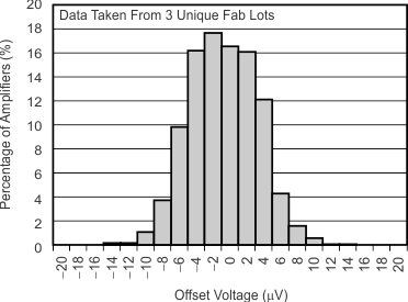
- Low Offset Voltage: 25 μV (Maximum)
- Zero-Drift: 0.03 μV/°C
- Low Noise: 8.8 nV/√Hz
- 0.1-Hz to 10-Hz Noise: 0.25 µVPP
- Excellent DC Precision:
- PSRR: 142 dB
- CMRR: 146 dB
- Open-Loop Gain: 136 dB
- Gain Bandwidth: 2 MHz
- Quiescent Current: 510 μA (Maximum)
- Wide Supply Range: ±2 V to ±18 V
- Rail-to-Rail Output
- Input Includes Negative Rail
- RFI Filtered Inputs
2 Applications
- HEV/EV Powertrain
- DC-DC Converters
- Traction Inverters
- Precision Safety and Sensing
(Braking, Position, and Passenger Occupancy Detection) - Precision Supervisory and Monitoring
3 Description
The OPAx188-Q1 operational amplifier family uses TI's proprietary zero drift techniques to provide low offset voltage (25-μV maximum) and near zero-drift over time and temperature. This miniature, high-precision, low-quiescent current amplifier family offers high input impedance and rail-to-rail output swing within 15 mV of the rails. The input common-mode range includes the negative rail. Either single or dual supplies can be used in the range from 4 V to 36 V (±2 V to ±18 V).
The OPA188-Q1 and OPA2188-Q1 are both offered in VSSOP-8. The single-channel version
(OPA188-Q1) is fully specified from –40°C to +125°C, and the dual-channel version (OPA2188-Q1) is fully specified from –40°C to +105°C.
Device Information(1)
| PART NUMBER | PACKAGE | BODY SIZE (NOM) |
|---|---|---|
| OPA188-Q1 | VSSOP (8) | 3.00 mm × 3.00 mm |
| OPA2188-Q1 |
- For all available packages, see the package option addendum at the end of the data sheet.
Offset Voltage Production Distribution
