SLVS033G February 1990 – July 2015 LT1054
PRODUCTION DATA.
- 1 Features
- 2 Applications
- 3 Description
- 4 Revision History
- 5 Pin Configuration and Functions
- 6 Specifications
- 7 Detailed Description
- 8 Application and Implementation
- 9 Power Supply Recommendations
- 10Layout
- 11Device and Documentation Support
- 12Mechanical, Packaging, and Orderable Information
Package Options
Refer to the PDF data sheet for device specific package drawings
Mechanical Data (Package|Pins)
- P|8
- DW|16
Thermal pad, mechanical data (Package|Pins)
- DW|16
Orderable Information
1 Features
2 Applications
- Industrial Communications (RS232)
- Data Acquisition Supply
- Voltage Inverters
- Voltage Regulators
- Negative Voltage Doublers
- Positive Voltage Doublers
3 Description
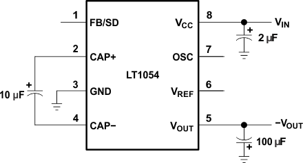
The LT1054 device is a bipolar, switched-capacitor voltage converter with regulator. It provides higher output current and significantly lower voltage losses than previously available converters. An adaptive-switch drive scheme optimizes efficiency over a wide range of output currents.
Total voltage drop at 100-mA output current typically is 1.1 V. This applies to the full supply-voltage range of 3.5 V to 15 V. Quiescent current typically is 2.5 mA.
The LT1054 also provides regulation, a feature previously not available in switched-capacitor voltage converters. By adding an external resistive divider, a regulated output can be obtained. This output is regulated against changes in both input voltage and output current. The LT1054 can also shut down by grounding the feedback terminal. Supply current in shutdown typically is 100 μA.
The internal oscillator of the LT1054 runs at a nominal frequency of 25 kHz. The oscillator terminal can be used to adjust the switching frequency or to externally synchronize the LT1054.
The LT1054C is characterized for operation over a free-air temperature range of 0°C to 70°C. The LT1054I is characterized for operation over a free-air temperature range of −40°C to 85°C.
Device Information(1)
| PART NUMBER | PACKAGE | BODY SIZE (NOM) |
|---|---|---|
| LT1054 | PDIP (8) | 9.50 mm × 6.35 mm |
| SOIC (16) | 10.30 mm × 10.30 mm |
- For all available packages, see the orderable addendum at the end of the data sheet.
Basic Voltage Inverter
