SNOSAI6J September 2005 – August 2016 LPV7215
PRODUCTION DATA.
- 1 Features
- 2 Applications
- 3 Description
- 4 Revision History
- 5 Pin Configuration and Functions
- 6 Specifications
- 7 Detailed Description
- 8 Application and Implementation
- 9 Power Supply Recommendations
- 10Layout
- 11Device and Documentation Support
- 12Mechanical, Packaging, and Orderable Information
Package Options
Mechanical Data (Package|Pins)
Thermal pad, mechanical data (Package|Pins)
Orderable Information
1 Features
2 Applications
- RC Timers
- Window Detectors
- IR Receivers
- Multivibrators
- Alarm and Monitoring Circuits
3 Description
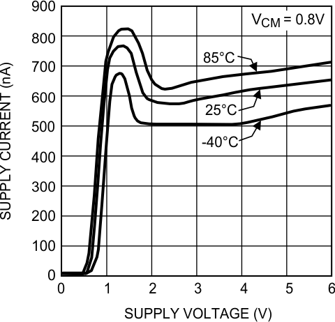
The LPV7215 device is an ultra-low-power comparator with a typical power supply current of
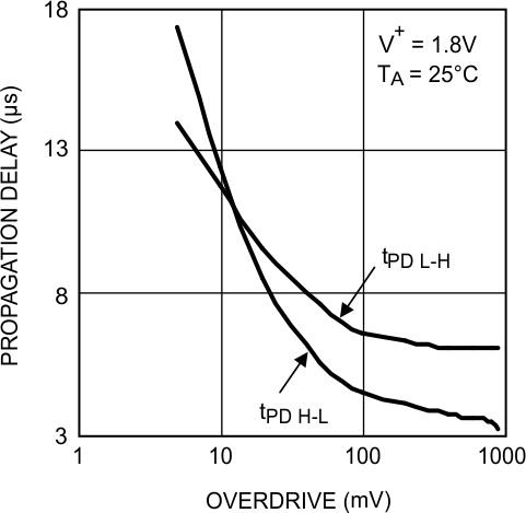
580 nA. It has the best-in-class power supply current versus propagation delay performance available among TI's low-power comparators. The propagation delay is as low as 4.5 µs with 100-mV overdrive at 1.8-V supply.
Designed to operate over a wide range of supply voltages, from 1.8 V to 5.5 V, with ensured operation at 1.8 V, 2.7 V, and 5 V, the LPV7215 is ideal for use in a variety of battery-powered applications. With rail-to-rail common-mode voltage range, the LPV7215 is well suited for single-supply operation.
Featuring a push-pull output stage, the LPV7215 allows for operation with absolute minimum power consumption when driving any capacitive or resistive load.
Available in a choice of space-saving packages, the LPV7215 is ideal for use in handheld electronics and mobile phone applications. The LPV7215 is manufactured with TI's advanced VIP50 process.
Device Information(1)
| PART NUMBER | PACKAGE | BODY SIZE (NOM) |
|---|---|---|
| LPV7215 | SOT-23 (5) | 2.90 mm × 1.60 mm |
| SC70 (5) | 2.00 mm × 1.25 mm |
- For all available packages, see the orderable addendum at the end of the data sheet.
Supply Current vs Supply Voltage

Propagation Delay vs Overdrive
