SNOSCY7 June 2014 LP2996A
PRODUCTION DATA.
- 1 Features
- 2 Applications
- 3 Description
- 4 Revision History
- 5 Pin Configuration and Functions
- 6 Specifications
- 7 Detailed Description
- 8 Applications and Implementation
- 9 Power Supply Recommendations
- 10Layout
- 11Device and Documentation Support
- 12Mechanical, Packaging, and Orderable Information
- 11Mechanical, Packaging, and Orderable Information
Package Options
Mechanical Data (Package|Pins)
- DDA|8
Thermal pad, mechanical data (Package|Pins)
- DDA|8
Orderable Information
1 Features
- 1.35V Minimum VDDQ
- Source and Sink Current
- Low Output Voltage Offset
- No External Resistors Required
- Linear Topology
- Suspend to Ram (STR) Functionality
- Low External Component Count
- Thermal Shutdown
- LP2998/8Q recommended for -40°C to 125°C
2 Applications
- DDR1, DDR2, DDR3, and DDR3L Termination Voltage
- FPGA
- Industrial/Medical PC
- SSTL-2 and SSTL-3 Termination
- HSTL Termination
3 Description
The LP2996A linear regulator is designed to meet the JEDEC SSTL-2 specifications for termination of DDR-SDRAM. The device also supports DDR2, DDR3 and DDR3L VTT bus termination with VDDQ min of 1.35V. The device contains a high-speed operational amplifier to provide excellent response to load transients. The output stage prevents shoot through while delivering 1.5A continuous current and transient peaks up to 3A in the application as required for DDR-SDRAM termination. The LP2996A also incorporates a VSENSE pin to provide superior load regulation and a VREF output as a reference for the chipset and DIMMs.
An additional feature found on the LP2996A is an active low shutdown (SD) pin that provides Suspend To RAM (STR) functionality. When SD is pulled low the VTT output will tri-state providing a high impedance output, but, VREF will remain active. A power savings advantage can be obtained in this mode through lower quiescent current.
Device Information(1)
| PART NUMBER | PACKAGE | BODY SIZE (NOM) |
|---|---|---|
| LP2996A | SO PowerPAD (8) | 4.89 mm x 3.90 mm |
- For all available packages, see the orderable addendum at the end of the datasheet.
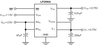
Simplified Schematic

4 Revision History
| DATE | REVISION | NOTES |
|---|---|---|
| June 2014 | * | Initial release. |