SNOSAT1I October 2006 – October 2017 LMV841 , LMV842 , LMV844
PRODUCTION DATA.
- 1 Features
- 2 Applications
- 3 Description
- 4 Revision History
- 5 Pin Configuration and Functions
- 6 Specifications
- 7 Detailed Description
- 8 Application and Implementation
- 9 Power Supply Recommendations
- 10Layout
- 11Device and Documentation Support
- 12Mechanical, Packaging, and Orderable Information
Package Options
Mechanical Data (Package|Pins)
Thermal pad, mechanical data (Package|Pins)
Orderable Information
1 Features
- Unless Otherwise Noted, Typical Values at
TA = 25 °C, V+ = 5 V. - Small 5-Pin SC70 Package (2.00 mm × 1.25 mm × 0.95 mm)
- Wide Supply Voltage Range: 2.7 V to 12 V
- Specified Performance at 3.3 V, 5 V and ±5 V
- Low Supply Current: 1 mA Per Channel
- Unity Gain Bandwidth: 4.5 MHz
- Open-Loop Gain: 133 dB
- Input Offset Voltage: 500 µV Maximum
- Input Bias Current: 0.3 pA
- CMRR at 112 dB and PSSR at 108 dB
- Input Voltage Noise: 20 nV/√Hz
- Temperature Range: −40°C to 125°C
- Rail-to-Rail Input and Output (RRIO)
2 Applications
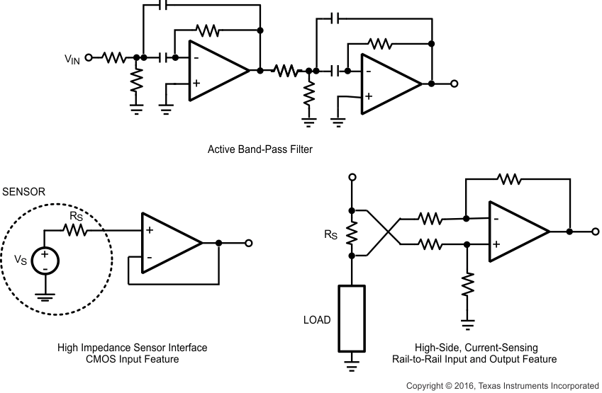
- High Impedance Sensor Interface
- Battery-Powered Instrumentation
- High Gain and Instrumentation Amplifiers
- DAC Buffers and Active Filters
3 Description
The LMV84x devices are low-voltage and low-power operational amplifiers that operate with supply voltages ranging from 2.7 V to 12 V and have rail-to-rail input and output capability. Their low offset voltage, low supply current, and CMOS inputs make them ideal for high impedance sensor interface and battery-powered applications.
The single LMV841 is offered in the space-saving 5-pin SC70 package, the dual LMV842 in the 8-pin VSSOP and 8-pin SOIC packages, and the quad LMV844 in the 14-pin TSSOP and 14-pin SOIC packages. These small packages are ideal solutions for area-constrained PCBs and portable electronics.
Device Information(1)
| PART NUMBER | PACKAGE | BODY SIZE (NOM) |
|---|---|---|
| LMV841 | SC70 (5) | 2.00 mm × 1.25 mm |
| LMV842 | VSSOP (8) | 3.00 mm × 3.00 mm |
| SOIC (8) | 4.90 mm × 3.91 mm | |
| LMV844 | SOIC (14) | 8.65 mm × 3.91 mm |
| TSSOP (14) | 5.00 mm × 4.40 mm |
- For all available packages, see the orderable addendum at the end of the data sheet.
Typical Applications
