SNOS998I February 2002 – October 2015 LMV761 , LMV762 , LMV762Q-Q1
PRODUCTION DATA.
- 1 Features
- 2 Applications
- 3 Description
- 4 Revision History
- 5 Pin Configuration and Functions
-
6 Specifications
- 6.1 Absolute Maximum Ratings
- 6.2 ESD Ratings: LMV761, LMV762
- 6.3 ESD Ratings: LMV762Q-Q1
- 6.4 Recommended Operating Conditions
- 6.5 Thermal Information
- 6.6 2.7-V Electrical Characteristics
- 6.7 5-V Electrical Characteristics
- 6.8 2-V Switching Characteristics
- 6.9 5-V Switching Characteristics
- 6.10 Typical Characteristics
- 7 Detailed Description
- 8 Application and Implementation
- 9 Power Supply Recommendations
- 10Layout
- 11Device and Documentation Support
- 12Mechanical, Packaging, and Orderable Information
Package Options
Mechanical Data (Package|Pins)
Thermal pad, mechanical data (Package|Pins)
Orderable Information
1 Features
- VS = 5 V, TA = 25°C, Typical Values Unless Specified
- Input Offset Voltage 0.2 mV
- Input Offset Voltage (Maximum Over Temp) 1 mV
- Input Bias Current 0.2 pA
- Propagation Delay (OD = 50 mV) 120 ns
- Low Supply Current 300 μA
- CMRR 100 dB
- PSRR 110 dB
- Extended Temperature Range −40°C to +125°C
- Push-Pull Output
- Ideal for 2.7-V and 5-V Single-Supply Applications
- Available in Space-Saving Packages:
- 6-Pin SOT-23 (Single With Shutdown)
- 8-Pin SOIC (Single With Shutdown)
- 8-Pin SOIC and VSSOP (Dual Without Shutdown)
- LMV762Q-Q1 is Qualified for Automotive Applications
- AEC-Q100 Qualified With the Following Results:
- Device Temperature Grade 1: –40°C to +125°C Ambient Operating Temperature Range
- Device HBM ESD Classification Level 1C
- Device CDM ESD Classification Level M2
2 Applications
- Portable and Battery-Powered Systems
- Scanners
- Set-Top Boxes
- High-Speed Differential Line Receiver
- Window Comparators
- Zero-Crossing Detectors
- High-Speed Sampling Circuits
- Automotive
3 Description
The LMV76x devices are precision comparators intended for applications requiring low noise and low input offset voltage. The LMV761 single has a shutdown pin that can be used to disable the device and reduce the supply current. The LMV761 is available in a space-saving 6-pin SOT-23 or 8-Pin SOIC package. The LMV762 dual is available in 8-pin SOIC or VSSOP package. The LMV762Q-Q1 is available VSSOP and SOIC packages.
These devices feature a CMOS input and push-pull output stage. The push-pull output stage eliminates the need for an external pullup resistor.
The LMV76x are designed to meet the demands of small size, low power and high performance required by portable and battery-operated electronics.
The input offset voltage has a typical value of 200 μV at room temperature and a 1-mV limit over temperature.
Device Information(1)
| PART NUMBER | PACKAGE | BODY SIZE (NOM) |
|---|---|---|
| LMV761 | SOIC (8) | 4.90 mm × 3.91 mm |
| SOT-23 (6) | 2.90 mm × 1.60 mm | |
| LMV762 LMV762Q-Q1 |
SOIC (8) | 4.90 mm × 3.91 mm |
| VSSOP (8) | 3.00 mm × 3.00 mm |
- For all available packages, see the orderable addendum at the end of the data sheet.
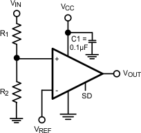
Threshold Detector

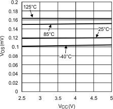
VOS vs VCC
