SNOSAI7K September 2005 – May 2016 LMV651 , LMV652 , LMV654
PRODUCTION DATA.
- 1 Features
- 2 Applications
- 3 Description
- 4 Revision History
- 5 Pin Configuration and Functions
- 6 Specifications
- 7 Detailed Description
- 8 Application and Implementation
- 9 Power Supply Recommendations
- 10Layout
- 11Device and Documentation Support
- 12Mechanical, Packaging, and Orderable Information
Package Options
Mechanical Data (Package|Pins)
- PW|14
Thermal pad, mechanical data (Package|Pins)
Orderable Information
1 Features
- Typical 5-V Supply, Unless Otherwise Noted
- Specified 3-V and 5-V Performance
- Low Power Supply Current
- LMV651: 116 μA
- LMV652: 118 μA per Amplifier
- LMV654: 122 μA per Amplifier
- High Unity-Gain Bandwidth: 12 MHz
- Maximum Input Offset Voltage: 1.5 mV
- CMRR: 100 dB
- PSRR: 95 dB
- Input Referred Voltage Noise: 17 nV/√Hz
- Output Swing With 2-kΩ Load, 120 mV from Rail
- Total Harmonic Distortion: 0.003% at 1 kHz, 2 kΩ
- Temperature Range: −40°C to 125°C
2 Applications
- Portable Equipment
- Automotive
- Battery-Powered Systems
- Sensors and Instrumentation
3 Description
TI’s LMV65x devices are high-performance, low-power operational amplifier ICs implemented with TI's advanced VIP50 process. This family of parts features 12 MHz of bandwidth while consuming only 116 μA of current, which is an exceptional bandwidth to power ratio in this operational amplifier class. The LMV65x devices are unity-gain stable and provide an excellent solution for general-purpose amplification in low-voltage, low-power applications.
This family of low-voltage, low-power amplifiers provides superior performance and economy in terms of power and space usage. These operational amplifiers have a maximum input offset voltage of 1.5 mV, a rail-to-rail output stage, and an input common-mode voltage range that includes ground. The LMV65x provide a PSRR of 95 dB, a CMRR of 100 dB, and a total harmonic distortion (THD) of 0.003% at 1-kHz frequency and 2-kΩ load.
The operating supply voltage range for this family of parts is from 2.7 V and 5.5 V. These operational amplifiers can operate over a wide temperature range (−40°C to 125°C), making them ideal for automotive applications, sensor applications, and portable equipment applications. The LMV651 is offered in the ultra-tiny 5-pin SC70 and 5-pin SOT-23 package. The LMV652 is offered in an 8-pin VSSOP package. The LMV654 is offered in a 14-pin TSSOP package.
Device Information(1)
| PART NUMBER | PACKAGE | BODY SIZE (NOM) |
|---|---|---|
| LMV651 | SOT-23 (5) | 2.90 mm × 1.60 mm |
| SC70 (5) | 2.00 mm × 1.25 mm | |
| LMV652 | VSSOP (8) | 3.00 mm × 3.00 mm |
| LMV654 | TSSOP (14) | 5.00 mm × 4.40 mm |
- For all available packages, see the orderable addendum at the end of the data sheet.
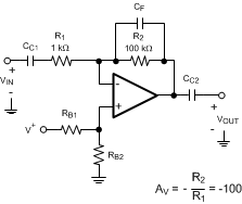
High Gain Wide Bandwidth Inverting Amplifier

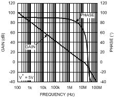
Open-Loop Gain and Phase vs Frequency
