SLOS447I September 2004 – May 2016 LMV341 , LMV342 , LMV344
PRODUCTION DATA.
- 1 Features
- 2 Applications
- 3 Description
- 4 Revision History
- 5 Pin Configuration and Functions
- 6 Specifications
- 7 Detailed Description
- 8 Application and Implementation
- 9 Power Supply Recommendations
- 10Layout
- 11Device and Documentation Support
- 12Mechanical, Packaging, and Orderable Information
Package Options
Refer to the PDF data sheet for device specific package drawings
Mechanical Data (Package|Pins)
- D|14
- PW|14
Thermal pad, mechanical data (Package|Pins)
Orderable Information
1 Features
- 2.7-V and 5-V Performance
- Rail-to-Rail Output Swing
- Input Bias Current:1 pA (Typical)
- Input Offset Voltage: 0.25 mV (Typical)
- Low Supply Current: 100 μA (Typical)
- Low Shutdown Current: 45 pA (Typical)
- Gain Bandwidth of 1 MHz (Typical)
- Slew Rate: 1 V/μs (Typical)
- Turnon Time From Shutdown: 5 μs (Typical)
- Input Referred Voltage Noise (at 10 kHz): 20 nV/√Hz
- ESD Protection Exceeds JESD 22
- 2000-V Human-Body Model (HBM)
- 750-V Charged-device model (CDM)
2 Applications
- Cordless and Cellular Phones
- Consumer Electronics (Laptops, PDAs)
- Audio Preamplifiers for Voice
- Portable, Battery-Powered Electronic Equipment
- Supply-Current Monitoring
- Battery Monitoring
- Buffers
- Filters
- Drivers
3 Description
The LMV34x devices are single, dual, and quad CMOS operational amplifiers, respectively, with low voltage, low power, and rail-to-rail output swing capabilities. The PMOS input stage offers an ultra-low input bias current of 1 pA (typical) and an offset voltage of 0.25 mV (typical). The single-supply amplifier is designed specifically for low-voltage
(2.7 V to 5 V) operation, with a wide common-mode input voltage range that typically extends from –0.2 V to 0.8 V from the positive supply rail. The LMV341 (single) also offers a shutdown (SHDN) pin that can be used to disable the device. In shutdown mode, the supply current is reduced to 33 nA (typical). Additional features of the family are a 20-nV/√Hz voltage noise at 10 kHz, 1-MHz unity-gain bandwidth, 1-V/μs slew rate, and 100-μA current consumption per channel.
Offered in both the SOT-23 and smaller SC70 packages, the LMV341 is suitable for the most space-constraint applications. The LMV342 dual device is offered in the standard SOIC and VSSOP packages. An extended industrial temperature range from –40°C to 125°C makes these devices suitable in a wide variety of commercial and industrial environments.
Device Information(1)
| PART NUMBER | PACKAGE | BODY SIZE (NOM) |
|---|---|---|
| LMV341IDCK | SC70 (6) | 2.00 mm × 1.25 mm |
| LMV341IDBV | SOT-23 (6) | 2.90 mm ×1.60 mm |
| LMV342ID | SOIC (8) | 4.90 mm × 3.91 mm |
| LMV342IDGK | VSSOP (8) | 3.00 mm × 3.00 mm |
| LMV344ID | SOIC (14) | 8.65 mm × 3.91 mm |
| LMV344IPW | TSSOP (14) | 5.00 mm × 4.40 mm |
- For all available packages, see the orderable addendum at the end of the data sheet.
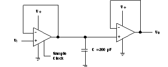
Sample-and-Hold Circuit
