SNOS990H April 2002 – June 2016 LMV341-N , LMV342-N , LMV344-N
PRODUCTION DATA.
- 1 Features
- 2 Applications
- 3 Description
- 4 Revision History
- 5 Pin Configuration and Functions
-
6 Specifications
- 6.1 Absolute Maximum Ratings
- 6.2 ESD Ratings
- 6.3 Recommended Operating Conditions
- 6.4 Thermal Information
- 6.5 Electrical Characteristics - 2.7 V (DC)
- 6.6 Electrical Characteristics - 2.7 V (AC)
- 6.7 Electrical Characteristics - 5 V (DC)
- 6.8 Electrical Characteristics - 5 V (AC)
- 6.9 Typical Characteristics
- 7 Detailed Description
- 8 Application and Implementation
- 9 Power Supply Recommendations
- 10Layout
- 11Device and Documentation Support
- 12Mechanical, Packaging, and Orderable Information
Package Options
Mechanical Data (Package|Pins)
Thermal pad, mechanical data (Package|Pins)
Orderable Information
1 Features
- Typical 2.7 V Supply Values (Unless Otherwise Noted)
- Ensured 2.7 V and 5 V Specifications
- Input Referred Voltage Noise at 10 kHz:
29 nV/√Hz - Supply Current (Per Amplifier): 100 µA
- Gain Bandwidth Product: 1 MHz
- Slew Rate: 1 V/µs
- Shutdown Current (LMV341-N): 45 pA
- Turnon Time From Shutdown (LMV341-N): 5 µs
- Input Bias Current: 20 fA
2 Applications
- Cordless or Cellular Phones
- Laptops
- PDAs
- PCMCIA or Audio
- Portable or Battery-Powered Electronic Equipment
- Supply Current Monitoring
- Battery Monitoring
- Buffers
- Filters
- Drivers
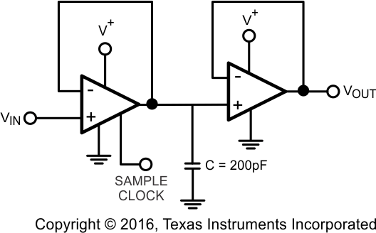
Sample and Hold Circuit

3 Description
The LMV34x-N devices are single, dual, and quad low-voltage, low-power operational amplifiers. They are designed specifically for low-voltage portable applications. Other important product characteristics are low input bias current, rail-to-rail output, and wide temperature range.
The patented class AB turnaround stage significantly reduces the noise at higher frequencies, power consumption, and offset voltage. The PMOS input stage provides the user with ultra-low input bias current of 20 fA (typical) and high input impedance.
The industrial-plus temperature range of −40°C to 125°C allows the LMV34x-N to accommodate a broad range of extended environment applications. LMV341-N expands Texas Instrument's Silicon Dust amplifier portfolio offering enhancements in size, speed, and power savings. The LMV34x-N devices are specified to operate over the voltage range of
2.7 V to 5.5 V and all have rail-to-rail output.
The LMV341-N offers a shutdown pin that can be used to disable the device. Once in shutdown mode, the supply current is reduced to 45 pA (typical). The LMV34x-N devices have 29-nV voltage noise at 10 KHz, 1 MHz GBW, 1-V/µs slew rate, 0.25 mVos, and 0.1-µA shutdown current (LMV341-N).
The LMV341-N is offered in the tiny 6-pin SC70 package, the LMV342-N in space-saving 8-pin VSSOP and SOIC packages, and the LMV344-N in 14-pin TSSOP and SOIC packages. These small package amplifiers offer an ideal solution for applications requiring minimum PCB footprint. Applications with area constrained PCB requirements include portable electronics such as cellular handsets and PDAs.
Device Information(1)
| PART NUMBER | PACKAGE | BODY SIZE (NOM) |
|---|---|---|
| LMV341-N | SC70 (6) | 2.00 mm × 1.25 mm |
| LMV342-N | VSSOP (8) | 3.00 mm × 3.00 mm |
| SOIC (8) | 4.90 mm × 3.91 mm | |
| LMV344-N | TSSOP (14) | 5.00 mm × 4.40 mm |
| SOIC (14) | 8.64 mm × 3.91 mm |
- For all available packages, see the orderable addendum at the end of the data sheet.
4 Revision History
Changes from G Revision (March 2013) to H Revision
- Added ESD Ratings table, Feature Description section, Device Functional Modes, Application and Implementation section, Power Supply Recommendations section, Layout section, Device and Documentation Support section, and Mechanical, Packaging, and Orderable Information sectionGo
- Changed Thermal Information tableGo
Changes from F Revision (March 2012) to G Revision
- Changed layout of National Data Sheet to TI formatGo