SNOSAW6E January 2008 – December 2014 LMP7721
PRODUCTION DATA.
- 1 Features
- 2 Applications
- 3 Description
- 4 Revision History
- 5 Pin Configuration and Functions
- 6 Specifications
- 7 Detailed Description
- 8 Application and Implementation
- 9 Power Supply Recommendations
- 10Layout
- 11Device and Documentation Support
- 12Mechanical, Packaging, and Orderable Information
Package Options
Mechanical Data (Package|Pins)
- D|8
Thermal pad, mechanical data (Package|Pins)
Orderable Information
1 Features
- Unless Otherwise Noted, Typical Values at TA = 25°C, VS = 5 V.
- Input Bias Current (VCM = 1 V)
- Maximum at 25°C ±20 fA
- Maximum at 85°C ±900 fA
- Offset Voltage ±26 µV
- Offset Voltage Drift −1.5 μV/°C
- DC Open-Loop Gain 120 dB
- DC CMRR 100 dB
- Input Voltage Noise (at f = 1 kHz) 6.5 nV/√Hz
- THD 0.0007%
- Supply Current 1.3 mA
- GBW 17 MHz
- Slew Rate (Falling Edge) 12.76 V/μs
- Supply Voltage 1.8 V to 5.5 V
- Operating Temperature Range −40°C to 125°C
- 8-Pin SOIC
2 Applications
- Photodiode Amplifier
- High Impedance Sensor Amplifier
- Ion Chamber Amplifier
- Electrometer Amplifier
- pH Electrode Amplifier
- Transimpedance Amplifier
Ultra-Low Input Bias Current

3 Description
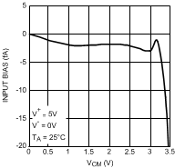
The LMP7721 is the industry’s lowest specified input bias current precision amplifier. The ultra-low input bias current is 3 fA, with a specified limit of ±20 fA at 25°C and ±900 fA at 85°C. This is achieved with the latest patent-pending technology of input bias current cancellation amplifier circuitry. This technology also maintains the ultra-low input bias current over the entire input common-mode voltage range of the amplifier.
Other outstanding features, such as low voltage noise (6.5 nV/√Hz), low DC-offset voltage (±150 µV maximum at 25°C) and low-offset voltage temperature coefficient (−1.5 µV/°C), improve system sensitivity and accuracy in high-precision applications. With a supply voltage range of 1.8 V to 5.5 V, the LMP7721 is the ideal choice for battery-operated, portable applications. The LMP7721 is part of the LMP™ precision amplifier family.
As part of Texas Instruments' PowerWise™ products, the LMP7721 provides the remarkably wide-gain bandwidth product (GBW) of 17 MHz while consuming only 1.3 mA of current. This wide GBW along with the high open-loop gain of 120 dB enables accurate signal conditioning. With these specifications, the LMP7721 has the performance to excel in a wide variety of applications such as electrochemical cell amplifiers and sensor interface circuits.
The LMP7721 is offered in an 8-pin SOIC package with a special pinout that isolates the amplifier’s input from the power supply and output pins. With proper board layout techniques, the unique pinout of the LMP7721 will prevent PCB leakage current from reaching the input pins. Thus system error will be further reduced.
Device Information(1)
| PART NUMBER | PACKAGE | BODY SIZE (NOM) |
|---|---|---|
| LMP7721 | SOIC (8) | 4.90 mm × 3.90 mm |
- For all available packages, see the orderable addendum at the end of the datasheet.