SNOSA71L October 2004 – September 2015 LMP2011 , LMP2012
PRODUCTION DATA.
- 1 Features
- 2 Applications
- 3 Description
- 4 Revision History
- 5 Pin Configuration and Functions
-
6 Specifications
- 6.1 Absolute Maximum Ratings
- 6.2 ESD Ratings
- 6.3 Recommended Operating Conditions
- 6.4 Thermal Information: LMP2011
- 6.5 Thermal Information: LMP2012
- 6.6 2.7-V DC Electrical Characteristics
- 6.7 2.7-V AC Electrical Characteristics
- 6.8 5-V DC Electrical Characteristics
- 6.9 5-V AC Electrical Characteristics
- 6.10 Typical Characteristics
- 7 Detailed Description
- 8 Application and Implementation
- 9 Power Supply Recommendations
- 10Layout
- 11Device and Documentation Support
- 12Mechanical, Packaging, and Orderable Information
Package Options
Mechanical Data (Package|Pins)
Thermal pad, mechanical data (Package|Pins)
Orderable Information
1 Features
- Low Ensured VOS Over Temperature 60 µV
- Low Noise with No 1/f 35nV/√Hz
- High CMRR 130 dB
- High PSRR 120 dB
- High AVOL 130 dB
- Wide Gain-Bandwidth Product 3 MHz
- High Slew Rate 4 V/µs
- Low Supply Current 930 µA
- Rail-to-Rail Output 30 mV
- No External Capacitors Required
(For VS = 5 V, Typical Unless Otherwise Noted)
2 Applications
- Precision Instrumentation Amplifiers
- Thermocouple Amplifiers
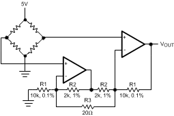
- Strain Gauge Bridge Amplifier
3 Description
The LMP201x series are the first members of TI's new LMP™ precision amplifier family. The LMP201x series offers unprecedented accuracy and stability in space-saving miniature packaging, offered at an affordable price. This device utilizes patented auto-zero techniques to measure and continually correct the input offset error voltage. The result is an amplifier which is ultra-stable over time and temperature. It has excellent CMRR and PSRR ratings, and does not exhibit the familiar 1/f voltage and current noise increase that plagues traditional amplifiers. The combination of the LMP201x characteristics makes it a good choice for transducer amplifiers, high gain configurations, ADC buffer amplifiers, DAC I-V conversion, and any other 2.7-V to 5-V application requiring precision and long term stability.
Other useful benefits of the LMP201x are rail-to-rail output, a low supply current of 930 µA, and wide gain-bandwidth product of 3 MHz. These versatile features found in the LMP201x provide high performance and ease of use.
Device Information(1)
| PART NUMBER | PACKAGE | BODY SIZE (NOM) |
|---|---|---|
| LMP2011 | SOIC (8) | 4.90 mm × 3.91 mm |
| SOT-23 (5) | 2.90 mm × 1.60 mm | |
| LMP2012 | SOIC (8) | 4.90 mm × 3.91 mm |
| VSSOP (8) | 3.00 mm × 3.00 mm |
- For all available packages, see the orderable addendum at the end of the data sheet.
Bridge Amplifier

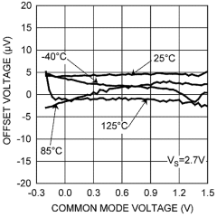
Offset Voltage vs Common Mode Voltage
