SNOSAV4B April 2008 – January 2016 LM7332
PRODUCTION DATA.
- 1 Features
- 2 Applications
- 3 Description
- 4 Revision History
- 5 Pin Configuration and Functions
- 6 Specifications
- 7 Detailed Description
- 8 Application and Implementation
- 9 Power Supply Recommendations
- 10Layout
- 11Device and Documentation Support
- 12Mechanical, Packaging, and Orderable Information
Package Options
Mechanical Data (Package|Pins)
Thermal pad, mechanical data (Package|Pins)
Orderable Information
1 Features
- VS = ±15 V, TA = 25°C, Typical Values Unless Specified
- Wide Supply Voltage Range 2.5 V to 32 V
- Wide Input Common Mode Voltage 0.3 V Beyond Rails
- Output Short Circuit Current > 100 mA
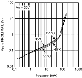
- High Output Current (1 V from Rails) ±70 mA
- GBWP 21 MHz
- Slew Rate 15.2 V/µs
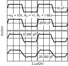
- Capacitive Load Tolerance Unlimited
- Total Supply Current 2 mA
- Temperature Range −40°C to +125°C
- Tested at −40°C, +125°C,
and +25°C at 5 V, ±5 V, ±15 V
2 Applications
- MOSFET and Power Transistor Driver
- Replaces Discrete Transistors in High Current Output Circuits
- Instrumentation 4–20 mA Current Loops
- Analog Data Transmission
- Multiple Voltage Power Supplies and Battery Chargers
- High-Side and Low-Side Current Sensing
- Bridge and Sensor Driving
- Digital-to-Analog Converter Output
3 Description
The LM7332 device is a dual rail-to-rail input and output amplifier with a wide operating temperature range (−40°C to +125°C) that meets the needs of automotive, industrial, and power supply applications. The LM7332 has an output current of 100 mA, which is higher than that of most monolithic operational amplifiers. Circuit designs with high output current requirements often require discrete transistors because many operational amplifiers have low current output. The LM7332 has enough current output to drive many loads directly, saving the cost and space of the discrete transistors.
The exceptionally wide operating supply voltage range of 2.5 V to 32 V alleviates any concerns over functionality under extreme conditions and offers flexibility of use in a multitude of applications. Most parameters of this device are insensitive to power supply variations; this design enhancement is another step in simplifying usage. Greater than rail-to-rail input common mode voltage range allows operation in many applications, including high-side and low-side sensing, without exceeding the input range.
The LM7332 can drive unlimited capacitive loads without oscillations.
The LM7332 is offered in the 8-pin VSSOP and SOIC packages.
Device Information(1)
| PART NUMBER | PACKAGE | BODY SIZE (NOM) |
|---|---|---|
| LM7332 | VSSOP (8) | 3.00 mm × 3.00 mm |
| SOIC (8) | 3.91 mm × 4.90 mm |
- For all available packages, see the orderable addendum at the end of the data sheet.
Output Swing vs Sourcing Current

Large Signal Step Response for Various Capacitive Loads
