SNVS963C SEPTEMBER 2013 – June 2016 LM5121 , LM5121-Q1
PRODUCTION DATA.
- 1 Features
- 2 Applications
- 3 Description
- 4 Revision History
- 5 Pin Configuration and Functions
- 6 Specifications
-
7 Detailed Description
- 7.1 Overview
- 7.2 Functional Block Diagram
- 7.3
Feature Description
- 7.3.1 Undervoltage Lockout (UVLO)
- 7.3.2 High Voltage VCC Regulator
- 7.3.3 Oscillator
- 7.3.4 Slope Compensation
- 7.3.5 Error Amplifier
- 7.3.6 PWM Comparator
- 7.3.7 Disconnection Switch Control
- 7.3.8 Soft-Start
- 7.3.9 HO and LO Drivers
- 7.3.10 Bypass Operation (VOUT = VIN)
- 7.3.11 Cycle-by-Cycle Current Limit
- 7.3.12 Circuit Breaker Function
- 7.3.13 Clock Synchronization
- 7.3.14 Maximum Duty Cycle
- 7.3.15 Thermal Protection
- 7.4 Device Functional Modes
-
8 Application and Implementation
- 8.1 Application Information
- 8.2
Typical Application
- 8.2.1 Design Requirements
- 8.2.2
Detailed Design Procedure
- 8.2.2.1 Timing Resistor RT
- 8.2.2.2 UVLO Divider RUV2, RUV1
- 8.2.2.3 Input Inductor LIN
- 8.2.2.4 Current Sense Resistor RS
- 8.2.2.5 Current Sense Filter RCSFP, RCSFN, CCS
- 8.2.2.6 Slope Compensation Resistor RSLOPE
- 8.2.2.7 Output Capacitor COUT
- 8.2.2.8 Input Capacitor CIN
- 8.2.2.9 VIN Filter RVIN, CVIN
- 8.2.2.10 Bootstrap Capacitor CBST and Boost Diode DBST
- 8.2.2.11 VCC Capacitor CVCC
- 8.2.2.12 Output Voltage Divider RFB1, RFB2
- 8.2.2.13 Soft-Start Capacitor CSS
- 8.2.2.14 Restart Capacitor CRES
- 8.2.2.15 Low-Side Power Switch QL
- 8.2.2.16 High-Side Power Switch QH and Additional Parallel Schottky Diode
- 8.2.2.17 Snubber Components
- 8.2.2.18 Disconnect Switch QD Selection
- 8.2.2.19 Freewheeling Diode DF Selection
- 8.2.2.20 Loop Compensation Components CCOMP, RCOMP, CHF
- 8.2.3 Application Curves
- 9 Power Supply Recommendations
- 10Layout
- 11Device and Documentation Support
- 12Mechanical, Packaging, and Orderable Information
Package Options
Mechanical Data (Package|Pins)
- PWP|20
Thermal pad, mechanical data (Package|Pins)
- PWP|20
Orderable Information
1 Features
-
AEC-Q100 Qualified with the following results:
- Device Temperature Grade 1: -40°C to +125°C Ambient Operating Temperature Range
- Device HBM ESD Classification Level 2
- Device CDM ESD Classification Level C6
- Maximum Input Voltage: 65 V
- Min Input Voltage: 3.0 V (4.5 V for startup)
- Output Voltage Up to 100 V
- Bypass (VOUT = VIN) Operation
- 1.2-V Reference with ±1.0% Accuracy
- Free-Run/Synchronizable up to 1 MHz
- Peak Current Mode Control
- Robust Integrated 3-A Gate Drivers
- Adaptive Dead-Time Control
- Optional Diode Emulation Mode
- Programmable Cycle-by-Cycle Current Limit
- Programmable Line UVLO
- Programmable Soft-Start
- Thermal Shutdown Protection
- Low Shutdown Quiescent Current: 9 μA
- Programmable Slope Compensation
- Programmable Skip Cycle Mode Reduces Standby Power
- Supports External VCC Bias Supply Option
- Load Disconnection in Shutdown Mode (True Shutdown)
- Inrush Current Limiting
- Hiccup Mode Short Circuit/Overload Protection
- Circuit Breaker Function
- Capable of Input Transient Suppression
- Capable of Reverse Battery Protection
- Thermally Enhanced 20-Pin HTSSOP
2 Applications
- 12-V, 24-V, and 48-V Power Systems
- Automotive Start-Stop
- High Current Boost Power Supply
- Battery Powered System
3 Description
The LM5121 is a synchronous boost controller intended for high-efficiency, high-power boost regulator applications. The control method is based upon peak current mode control. Current mode control provides inherent line feed-forward, cycle-by-cycle current limiting and ease of loop compensation.
The switching frequency is programmable up to 1 MHz. Higher efficiency is achieved using two robust N-channel MOSFET gate drivers with adaptive dead-time control. A user-selectable diode emulation mode enables discontinuous mode operation for improved efficiency at light load conditions.
The LM5121 provides disconnection switch control which completely disconnects the output from the input during an output short or a shutdown condition. During start-up sequence, inrush current is limited by the disconnection switch control.
An internal charge pump allows 100% duty cycle operation of the high-side synchronous switch (Bypass operation). Additional features include thermal shutdown, frequency synchronization, hiccup mode current limit and adjustable line undervoltage lockout.
Device Information(1)
| PART NUMBER | PACKAGE | BODY SIZE (NOM) |
|---|---|---|
| LM5121 | HTSSOP (20) | 6.50 mm x 4.40 mm |
| LM5121-Q1 |
- For all available packages, see the orderable addendum at the end of the datasheet.
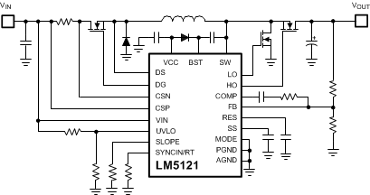
Simplified Application Diagram
