SNVS300H July 2004 – September 2016 LM5111
PRODUCTION DATA.
- 1 Features
- 2 Applications
- 3 Description
- 4 Revision History
- 5 Device Options
- 6 Pin Configuration and Functions
- 7 Specifications
- 8 Detailed Description
- 9 Application and Implementation
- 10Power Supply Recommendations
- 11Layout
- 12Device and Documentation Support
- 13Mechanical, Packaging, and Orderable Information
Package Options
Mechanical Data (Package|Pins)
Thermal pad, mechanical data (Package|Pins)
- DGN|8
Orderable Information
1 Features
- Independently Drives Two N-Channel MOSFETs
- Compound CMOS and Bipolar Outputs Reduce Output Current Variation
- 5-A Sink and 3-A Source Current Capability
- Two Channels can be Connected in Parallel to Double the Drive Current
- Independent Inputs (TTL Compatible)
- Fast Propagation Times (25 ns Typical)
- Fast Rise and Fall Times (14 ns and 12 ns Rise and Fall, Respectively, With 2-nF Load)
- Available in Dual Noninverting, Dual Inverting and Combination Configurations
- Supply Rail Undervoltage Lockout Protection (UVLO)ƒ
- LM5111-4 UVLO Configured to Drive PFET through OUT_A and NFET through OUT_B
- Pin Compatible With Industry Standard Gate Drivers
2 Applications
- Synchronous Rectifier Gate Drivers
- Switch-mode Power Supply Gate Driver
- Solenoid and Motor Drivers
3 Description
The LM5111 Dual Gate Driver replaces industry standard gate drivers with improved peak output current and efficiency. Each compound output driver stage includes MOS and bipolar transistors operating in parallel that together sink more than 5-A peak from capacitive loads. Combining the unique characteristics of MOS and bipolar devices reduces drive current variation with voltage and temperature. Undervoltage lockout protection is also provided. The drivers can be operated in parallel with inputs and outputs connected to double the drive current capability. This device is available in the SOIC package or the thermally enhanced
MSOP-PowerPAD package.
Device Information(1)
| PART NUMBER | PACKAGE | BODY SIZE (NOM) |
|---|---|---|
| LM5111 | SOIC (8) | 5.00 mm x 6.00 mm |
| MSOP-PowerPAD (8) | 3.00 mm x 4.90 mm |
- For all available packages, see the orderable addendum at the end of the data sheet.
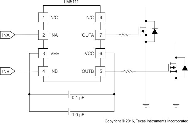
Simplified Application Diagram
