SNVS565I November 2008 – August 2015 LM5085 , LM5085-Q1
PRODUCTION DATA.
- 1 Features
- 2 Applications
- 3 Description
- 4 Revision History
- 5 Pin Configuration and Functions
- 6 Specifications
- 7 Detailed Description
- 8 Application and Implementation
- 9 Power Supply Recommendations
- 10Layout
- 11Device and Documentation Support
- 12Mechanical, Packaging, and Orderable Information
Package Options
Refer to the PDF data sheet for device specific package drawings
Mechanical Data (Package|Pins)
- DGN|8
Thermal pad, mechanical data (Package|Pins)
- DGN|8
Orderable Information
1 Features
- LM5085-Q1 is an Automotive Grade Product that is AEC-Q100 Grade 1 Qualified (–40°C to 125°C Operating Junction Temperature)
- Wide 4.5-V to 75-V Input Voltage Range
- Adjustable Current Limit Using RDS(ON) or a Current Sense Resistor
- Programmable Switching Frequency to 1MHz
- No Loop Compensation Required
- Ultra-Fast Transient Response
- Nearly Constant Operating Frequency with Line and Load Variations
- Adjustable Output Voltage from 1.25 V
- Precision ±2% Feedback Reference
- Capable of 100% Duty Cycle Operation
- Internal Soft-start Timer
- Integrated High Voltage Bias Regulator
- Thermal Shutdown
- Package:
- HVSSOP-8
- VSSOP-8
- WSON-8
2 Applications
- Automotive Infotainment
- Battery/Super Capacitor Chargers
- LED Drivers
3 Description
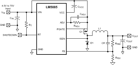
The LM5085 is a high efficiency PFET switching regulator controller that can be used to quickly and easily develop a small, efficient buck regulator for a wide range of applications. This high voltage controller contains a PFET gate driver and a high voltage bias regulator which operates over a wide 4.5-V to 75-V input range. The constant on-time regulation principle requires no loop compensation, simplifies circuit implementation, and results in ultrafast load transient response. The operating frequency remains nearly constant with line and load variations due to the inverse relationship between the input voltage and the on-time. The PFET architecture allows 100% duty cycle operation for a low dropout voltage. Either the RDS(ON) of the PFET or an external sense resistor can be used to sense current for over-current detection.
Device Information(1)
| PART NUMBER | PACKAGE | BODY SIZE (NOM) |
|---|---|---|
| LM5085 | VSSOP (8) | 3.00 mm x 3.00 mm |
| HVSSOP (8) | ||
| WSON (8) | ||
| LM5085-Q1 | HVSSOP (8) | 3.00 mm x 3.00 mm |
- For all available packages, see the orderable addendum at the end of the datasheet.
Typical Application, Basic Step Down Controller
