SNVSA36C April 2014 – October 2017 LM43602
PRODUCTION DATA.
- 1 Features
- 2 Applications
- 3 Description
- 4 Revision History
- 5 Pin Configuration and Functions
- 6 Specifications
-
7 Detailed Description
- 7.1 Overview
- 7.2 Functional Block Diagram
- 7.3
Feature Description
- 7.3.1 Fixed Frequency Peak Current-Mode Controlled Step-Down Regulator
- 7.3.2 Light Load Operation
- 7.3.3 Adjustable Output Voltage
- 7.3.4 Enable (EN)
- 7.3.5 VCC, UVLO and BIAS
- 7.3.6 Soft-Start and Voltage Tracking (SS/TRK)
- 7.3.7 Switching Frequency (RT) and Synchronization (SYNC)
- 7.3.8 Minimum ON-time, Minimum OFF-time and Frequency Foldback at Drop-Out Conditions
- 7.3.9 Internal Compensation and CFF
- 7.3.10 Bootstrap Voltage (BOOT)
- 7.3.11 Power Good (PGOOD)
- 7.3.12 Over Current and Short Circuit Protection
- 7.3.13 Thermal Shutdown
- 7.4 Device Functional Modes
-
8 Applications and Implementation
- 8.1 Application Information
- 8.2
Typical Applications
- 8.2.1 Design Requirements
- 8.2.2
Detailed Design Procedure
- 8.2.2.1 Custom Design With WEBENCH® Tools
- 8.2.2.2 Output Voltage Set-Point
- 8.2.2.3 Switching Frequency
- 8.2.2.4 Input Capacitors
- 8.2.2.5 Inductor Selection
- 8.2.2.6 Output Capacitor Selection
- 8.2.2.7 Feed-Forward Capacitor
- 8.2.2.8 Bootstrap Capacitors
- 8.2.2.9 VCC Capacitor
- 8.2.2.10 BIAS Capacitors
- 8.2.2.11 Soft-Start Capacitors
- 8.2.2.12 Under Voltage Lockout Set-Point
- 8.2.2.13 PGOOD
- 8.2.3 Application Performance Curves
- 9 Power Supply Recommendations
- 10Layout
- 11Device and Documentation Support
- 12Mechanical, Packaging, and Orderable Information
Package Options
Refer to the PDF data sheet for device specific package drawings
Mechanical Data (Package|Pins)
- PWP|16
- DSU|16
Thermal pad, mechanical data (Package|Pins)
- PWP|16
Orderable Information
1 Features
- 27-µA Quiescent Current in Regulation
- High Efficiency at Light Load (DCM and PFM)
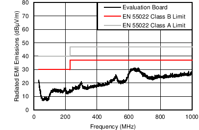
- Meets EN55022/CISPR 22 EMI standards
- Integrated Synchronous Rectification
- Adjustable Frequency Range: 200 kHz to 2.2 MHz (500 kHz Default)
- Frequency Synchronization to External Clock
- Internal Compensation
- Stable with Almost Any Combination of Ceramic, Polymer, Tantalum, and Aluminum Capacitors
- Power-Good Flag
- Soft-Start into a Pre-Biased Load
- Internal Soft Start: 4.1 ms
- Extendable Soft-Start Time by External Capacitor
- Output Voltage Tracking Capability
- Precision Enable to Program System UVLO
- Output Short Circuit Protection with Hiccup Mode
- Overtemperature Thermal Shutdown Protection
- Create a Custom Design Using the LM43602 with the WEBENCH® Power Designer
2 Applications
- Industrial Power Supplies
- Telecommunications Systems
- Sub-AM Band Automotive
- General Purpose Wide VIN Regulation
- High Efficiency Point-Of-Load Regulation
space
3 Description
The LM43602 regulator is an easy-to-use synchronous step-down DC-DC converter capable of driving up to 2 A of load current from an input voltage ranging from 3.5 V to 36 V (42-V absolute maximum). The LM43602 provides exceptional efficiency, output accuracy, and dropout voltage in a very small solution size. An extended family is available in 0.5-A, 1-A, and 3-A load current options in pin-to-pin compatible packages. Peak current-mode control is employed to achieve simple control loop compensation and cycle-by-cycle current limiting. Optional features such as programmable switching frequency, synchronization, power-good flag, precision enable, internal soft start, extendable soft start, and tracking provide a flexible and easy-to-use platform for a wide range of applications. Discontinuous conduction and automatic frequency modulation at light loads improve light-load efficiency. The family requires few external components and terminal arrangement allows simple, optimum PCB layout. Protection features include thermal shutdown, VCC undervoltage lockout, cycle-by-cycle current limit, and output short circuit protection. The LM43602 device is available in a 16-lead HTSSOP package (5.1 mm × 6.6 mm × 1.2 mm) and 16-pin VSON package with wettable flanks.
Device Information
| ORDER NUMBER | PACKAGE | BODY SIZE |
|---|---|---|
| LM43602 | HTSSOP (16) | 5.10 mm × 6.60 mm |
| VSON (16) | 4.10 mm × 5.10 mm |
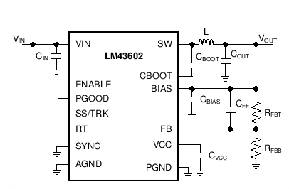
Simplified Schematic

LM43602PWPEVM Radiated Emission Graph
12VIN to 3.3 VOUT,
FS = 500 kHz, IOUT = 2 A
