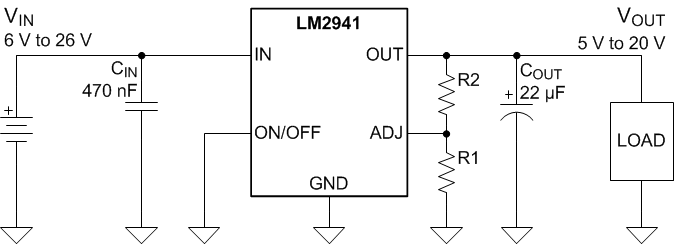
SNVS770I June 1999 – January 2015 LM2941 , LM2941C
PRODUCTION DATA.
- 1 Features
- 2 Applications
- 3 Description
- 4 Revision History
- 5 Pin Configuration and Functions
- 6 Specifications
- 7 Detailed Description
- 8 Application and Implementation
- 9 Power Supply Recommendations
- 10Layout
- 11Device and Documentation Support
- 12Mechanical, Packaging, and Orderable Information
Package Options
Refer to the PDF data sheet for device specific package drawings
Mechanical Data (Package|Pins)
- NDH|5
- NGN|8
- KTT|5
- KC|5
Thermal pad, mechanical data (Package|Pins)
- KTT|5
Orderable Information
1 Features
- Operating VIN Range: 6 V to 26 V
- Output Voltage Adjustable From 5 V to 20 V
- Dropout Voltage Typically 0.5 V at IOUT = 1 A
- Output Current in Excess of 1 A
- Trimmed Reference Voltage
- Reverse Battery Protection
- Internal Short-Circuit Current Limit
- Mirror Image Insertion Protection
- P+ Product Enhancement Tested
- TTL, CMOS Compatible ON/OFF Switch
- WSON Space-Saving Package
2 Applications
- Industrial
- Automotive
3 Description
The LM2941 positive voltage regulator features the ability to source 1 A of output current with a typical dropout voltage of 0.5 V and a maximum of 1 V over the entire temperature range. Furthermore, a quiescent current reduction circuit has been included which reduces the ground pin current when the differential between the input voltage and the output voltage exceeds approximately 3 V. The quiescent current with 1 A of output current and an input-output differential of 5 V is therefore only 30 mA. Higher quiescent currents only exist when the regulator is in the dropout mode (VIN − VOUT ≤ 3 V).
Designed also for vehicular applications, the LM2941 and all regulated circuitry are protected from reverse battery installations or two-battery jumps. During line transients, such as load dump when the input voltage can momentarily exceed the specified maximum operating voltage, the regulator will automatically shut down to protect both the internal circuits and the load. Familiar regulator features such as short circuit and thermal overload protection are also provided.
Device Information(1)
| PART NUMBER | PACKAGE | BODY SIZE (NOM) |
|---|---|---|
| LM2941 | WSON (8) | 4.00 mm x 4.00 mm |
| TO-263 (5) | 10.16 mm x 8.42 mm | |
| TO-220 (5) | 14.986 mm x 10.16 mm | |
| TO-220 (5) | 10.16 mm x 8.51 mm | |
| LM2941C | TO-263 (5) | 10.16 mm x 8.42 mm |
| TO-220 (5) | 14.986 mm x 10.16 mm | |
| TO-220 (5) | 10.16 mm x 8.51 mm |
- For all available packages, see the orderable addendum at the end of the datasheet.
