TIDT238 July   2021 TL7700-SEP


  1. 1Description
  2. 2Test Prerequisites
    1. 2.1 Voltage and Current Requirements
    2. 2.2 Considerations
    3. 2.3 Dimensions
  3. 3Testing and Results
    1. 3.1 Efficiency Graphs
    2. 3.2 Efficiency Data
    3. 3.3 Thermal Images
    4. 3.4 EMI
  4. 4Waveforms
    1. 4.1 Switching
    2. 4.2 Output Voltage Ripple
    3. 4.3 Load Transients
    4. 4.4 Start-up Sequence

Description

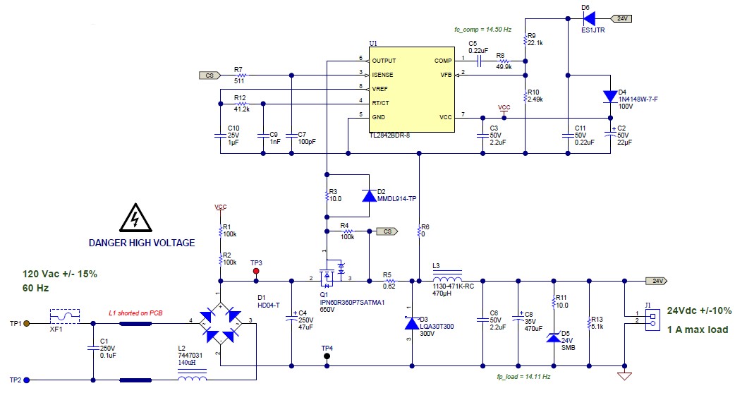
This reference design uses a TL2842B as a high-side buck to convert a 120-VAC input to a 24-VDC output capable of 1-A loading. At full load it achieves a low peak-to-peak output ripple and over 88% efficiency at full load. This reference design was built using a 2-layer PCB and single-sided assembly.
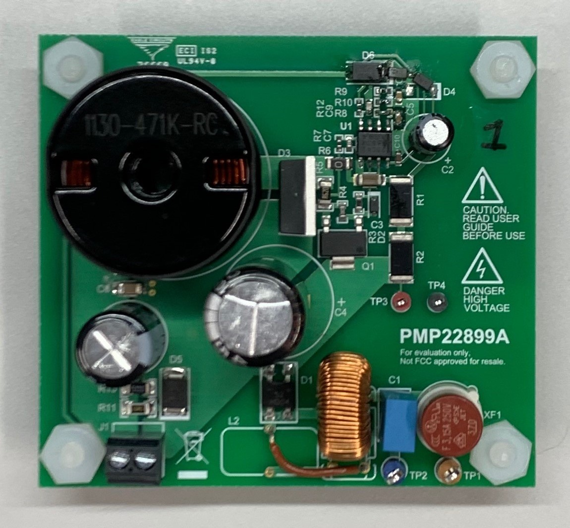
GUID-20210428-CA0I-MGW7-DTFC-M9FR2XQ2R10R-low.pngFigure 1-1 PCB Top
GUID-20210428-CA0I-W0ZN-BK3X-TMW1BVFZ2Q7C-low.pngFigure 1-2 Schematic